Introduction
Welcome to the MSP430 ADC academy. This lab demonstrates how to use the MSP430 built-in ADC module to convert analog voltage signal to digital data which can be used for control processes. Several ADC conversion modes will be demonstrated. This lab uses MSP430Ware register level code examples from MSP430Ware.
The lab has 3 tasks consisting of the following activities:
- Sample analog input with Single-Channel Single-Conversion Mode, light LED if the analog input voltage is > 0.5V.
- Sample three analog inputs with Repeat-Sequence-of-Channels Mode and store the conversion results into an array.
- ADC Window Comparator to monitor analog input voltage. Toggle LED with different frequencies according to different analog voltage ranges.
Prerequisites
Hardware
The following hardware is required for this lab
Software
The following software is required for this lab
Installing the software
NOTE:
The software examples used for this lab should be imported from within the TI Resource Explorer. This can be accessed from the web or locally in CCS by clicking View→Resource Explorer. Before importing a Project, you first need to download MSP430Ware to be able to import the examples to the CCS IDE. This may be done when CCS was installed or can be done later by clicking the "Download and Install" icon in the top right. Note that installing MSP430Ware for any project will install ALL labs and content, so this only needs to be done once.
Recommended Resources
The training videos provide a fundamental ADC parameter introduction, ADC peripherals in MSP430FR2x/4x/5/6x devices. The documentation can be referenced for the MSP430 MCU and ADC details.
- ADC DC Specifications – INL, DNL, Cin, Leakage, Vref
- AC & DC Specifications – Offset Error, Gain Error, CMRR, PSRR, SNR, and THD
- MSP430FR4x/FR2x MCUS Key Peripherals
- MSP-EXP430FR5969 Workshop - Part 5: MSP430FR5969 ADC12_B
- ADC wake and transmit on threshold
- MSP430FR2433 MCU Datasheet
- MSP430FR4xx_2xx MCU UserGuide
- Designing With the MSP430FR4xx and MSP430FR2xx ADC
- Designing With MSP430FR58xx/FR59xx/68xx/69xx ADC
- MSP430 MCUs Development Guide Book (Search ADC for ADC related application report, and CCS for how to set up CCS IDE)
Overview
In this lab, you will be using one LaunchPad and input an analog voltage signal into the LaunchPad header pins which have ADC input function.
You will see the ADC conversion results in the ADC result registers and you will also see the LED blink with different frequencies according to the input analog voltages.
Getting Started
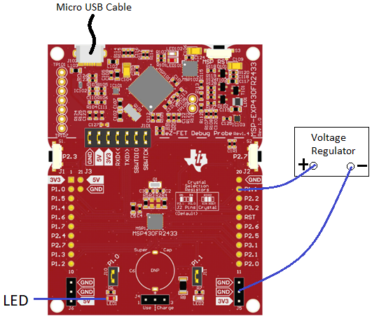
Hardware Setup:
To connect the MSP430 launch pads for ADC conversion test:
- Connect the USB cable to LaunchPad for power supply, programming, and debugging
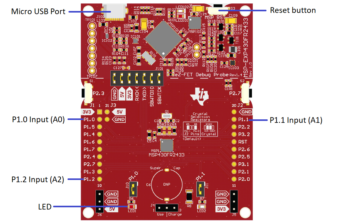
- Input P1.1 pin (J2.19 of LaunchPad) with analog signal less than 3.6v which is the maximum operation voltage of MSP430FR2433.
- Input P1.3 pin (J1.9 of LaunchPad), P1.2 pin (J1.10 of LaunchPad) with analog signals less than 3.6v.
Launchpad Input and Output diagram:
Task 1 – Sample Analog Input with Single-Channel Single-Conversion Mode
Task 1 Example Project Overview
This task is to sample an analog input, turn on the LED if the analog input voltage is greater than 0.5V, and turn off the LED if the input voltage is less than 0.5V. The purpose is to demonstrate how to use the ADC Single-Channel Single-Conversion Mode to convert analog input to digital data.
In this task there is no code to modify. So build and program the msp430 LaunchPad with the code example
- Import the adc_02.c example msp430fr243x_adc10_02.c into CCS from TI Resource Explorer.
MSP430ware→Development Tools→MSP-EXP430FR2433→Peripheral Examples→Register Level→MSP430FR2433→
msp430fr243x_adc10_02.c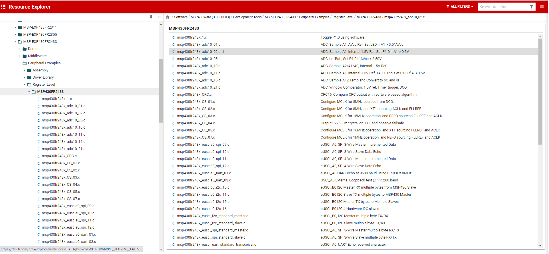
- Click Import in the upper right-hand corner
- Build the code and program it to the LaunchPad.
Task 1 Code Overview
Let us break down the MSP430 example code into three parts:
- Initialization
- Main loop
- ADC subroutine
Initialization:
In this code example, the following modules are used: Watchdog, clock system (for CPU and ADC), GPIO, ADC module, and voltage reference. These modules need to be configured before the main loop code execution.
The Watchdog module should be disabled to prevent the watchdog timer from triggering a reset while the example code is running.
WDTCTL = WDTPW | WDTHOLD; // Stop WDTSince the code example is using the default clock frequency after power-on, there is no code for clock system configuration.
Default CPU clock is MCLK = SMCLK = default DCODIV ~1MHz. Low frequency peripheral clock ACLK = default REFO ~32768Hz. ADC dedicated clock MODCLK = ~5MHz.
GPIO initialization is to configure the package pins to assgined functionalities: GPIO output, ADC input. After the GPIO initialization, unlock the GPIO high-impedance mode by resetting the LOCKLPM5 bit.
In this example code, port P1.0 is configured to output. ADC input pin A1 (shared with port P1.1) is selected for analog signal input. Please note, the input analog signal should be less than 3.6V.
ADC module initialization is to configure ADC related registers: sample-and-hold time and source, simpling signal (SAMPCON) select, ADC clock source, conversion mode, ADC resolution, interrupt enable, ADC conversion start source.
In this example code, ADCCLK is set to MODCLK and 16 ADCCLK (MODCLK) cycles setting is selected for sample-and-hold time (see ADCCTL0.ADCSHT), sample-and-hold start signal SAMPCON is set from sampling timer (see ADCCTL1.ADCSHP), conversion mode is set to Single-channel Single-conversion mode (see ADCCTL1.ADCCONSEQ), 10bit resolution is configured (see ADCCTL2.ADCRES), ADC conversion completed interrupt is enabled (see ADCIE.ADCIE0) and ADC conversion start source is software trigger ADCCTL1.ADCSC bit.
Configure the voltage reference for the ADC module. In this code example, the internal reference 1.5V is selected as the ADC conversion voltage reference.
 // Configure GPIO
 P1DIR |= BIT0;                                            // Set P1.0/LED to output direction
 P1OUT &= ~BIT0;                                           // P1.0 LED off

 // Configure ADC A1 pin, shared with P1.1
 SYSCFG2 |= ADCPCTL1;

 // Disable the GPIO power-on default high-impedance mode to activate
 // previously configured port settings
 PM5CTL0 &= ~LOCKLPM5;

 // Configure ADC10
 ADCCTL0 |= ADCSHT_2 | ADCON;                              // ADCON, S&H=16 ADC clks
 ADCCTL1 |= ADCSHP;                                        // ADCCLK = MODOSC; sampling timer; ADC conversion start source is ADCSC bit
 ADCCTL2 |= ADCRES;                                        // 10-bit conversion results
 ADCIE |= ADCIE0;                                          // Enable ADC conv complete interrupt
 ADCMCTL0 |= ADCINCH_1 | ADCSREF_1;                        // A1 ADC input select; Vref is internal 1.5V

 // Configure voltage reference for ADC conversion
 PMMCTL0_H = PMMPW_H;                                      // Unlock the PMM registers
 PMMCTL2 |= INTREFEN;                                      // Enable internal reference 1.5V
 __delay_cycles(400);                                      // Delay for reference settling
Configure ADC trigger source. In this code example, the ADC trigger source is the default ADCSC.
Main loop:
In this code example, the main loop function is simple.
Trigger the ADC sample-and-conversion start, entering low power mode LPM0, wait for interrupt to exit LPM0 to execute next lines of code.
Turn on the LED if the analog input voltage is greater than 0.5V and turn off the LED if the input voltage is less than 0.5V.
The 0x155 is the ADC conversion result of 0.5V with internal reference 1.5V as ADC voltage reference.
while(1)
{
   ADCCTL0 |= ADCENC | ADCSC;                            // Sampling and conversion start
   __bis_SR_register(LPM0_bits | GIE);                   // LPM0, ADC_ISR will force exit
   if (ADC_Result < 0x155)                               // 0.5v = 1.5v* 0x155/0x3ff
       P1OUT &= ~BIT0;                                   // Clear P1.0 LED off
   else
       P1OUT |= BIT0;                                    // Set P1.0 LED on
   __delay_cycles(5000);
}
ADC subroutine:
In this code example, the ADC interrupt request will be triggered when the ADC conversion is completed.
MCU works in low power mode LPM0. After ADC conversion is completed, the ADC interruption will be triggered.
In the ADC subroutine, the ADC conversion result is stored in variable named
ADC_Result. The CPU exits the low-power mode LPM0 and code execution is continued in the main loop where the ADC conversion result to turn on or turn off the LED can be processed.// ADC interrupt service routine #if defined(__TI_COMPILER_VERSION__) || defined(__IAR_SYSTEMS_ICC__) #pragma vector=ADC_VECTOR __interrupt void ADC_ISR(void) #elif defined(__GNUC__) void __attribute__ ((interrupt(ADC_VECTOR))) ADC_ISR (void) #else #error Compiler not supported! #endif { switch(__even_in_range(ADCIV,ADCIV_ADCIFG)) { case ADCIV_NONE: break; case ADCIV_ADCOVIFG: break; case ADCIV_ADCTOVIFG: break; case ADCIV_ADCHIIFG: break; case ADCIV_ADCLOIFG: break; case ADCIV_ADCINIFG: break; case ADCIV_ADCIFG: ADC_Result = ADCMEM0; __bic_SR_register_on_exit(LPM0_bits); // Clear CPUOFF bit from LPM0 break; default: break; } }
Task 1 Code Execution
Connect the PC and LaunchPad with a Micro USB cable. In CCS, build the example code and program the LaunchPad. Input the analog voltage signal (using an adjustable voltage regulator) on the header pin P1.1 (J2.19). (Please note the external voltage should be applied on P1.1 after the MCU DVCC power-on.)
After the LaunchPad reset, the code will execute. You can see the LED turn on if the voltage on the A1 input is greater or equal to 0.5V, or the LED is turned off if the voltage on the A1 input is less than 0.5V. Vary the voltage on pin P1.1 to see if the LaunchPad works as exptected or not.
What description is correct for MSP430FR2433?
Task 2 – Sample Three Analog Inputs with Repeat-Sequence-of-Channels Mode
Task 2 Example Project Overview
The purpose of this task is to introduce ADC Repeat-Sequence-of-Channels mode functionality on the MSP430.
In the example code, the ADC will sample inputs A2, A1, A0 and store the conversion results in array varaible ADC_Result[3].
The trigger signal is timer_A output signal TA1.1B, which is connected to the ADC module.
- Import the adc_10.c example msp430fr243x_adc10_10.c into CCS from TI Resource Explorer.
MSP430ware→Development Tools→MSP-EXP430FR2433→Peripheral Examples→Register Level→MSP430FR2433→
msp430fr243x_adc10_10.c- Click import in the upper right-hand corner
- Build the code and program it to the LaunchPad.
Task 2 Code Overview
Same as Task #1, let us break down the MSP430 example code into three parts:
- Initialization
- Main loop
- ADC subroutine
Initialization:
In this code example, the ollowing modules are used: Watchdog, clock system (for CPU and ADC), GPIO, ADC module, voltage reference, and TA1. These modules need to be configured before the main loop code execution.
The Watchdog module should be disabled to prevent the watchdog timer from triggering a reset while the example code is running.
Since the code example is using the default clock frequency after power-on, there is no code for clock system configuration.
Default CPU clock is MCLK = SMCLK = default DCODIV ~1MHz. Low frequency peripheral clock ACLK = default REFO ~32768Hz. ADC dedicated clock MODCLK = ~5MHz.
GPIO initialization configures the package pins to assigned functionalities: GPIO output, and ADC input. After the GPIO initialization, unlock the GPIO high-impedance mode by resetting LOCKLPM5 bit.
In this example code, port P1.0, P1.1, P1.2 are configured to ADC function A0, A1, A2. Please note, the input analog signal should be less than 3.6V.
ADC module initialization is to configure ADC related registers: sample-and-hold time and source, sampling signal (SAMPCON) select, ADC clock source, conversion mode, ADC resolution, interrupt enable, ADC sample-and-conversion trigger source.
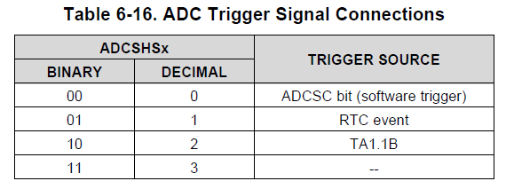
In this example code, ADCCLK is set to MODCLK and 16 ADCCLK (MODCLK) cycles setting is selected for sample-and-hold time (see ADCCTL0.ADCSHT), sample-and-hold start signal SAMPCON source is set from sampling timer (see ADCCTL1.ADCSHP), conversion mode is set to Repeat-Sequence-of-Channels mode (see ADCCTL1.ADCCONSEQ), 8bit resolution is configured (see ADCCTL2.ADCRES), ADC conversion completed interrupt is enabled (see ADCIE.ADCIE0) and ADC sample-and-conversion trigger source is set as TA1.1B (see ADCCTL1.ADCSHS). You can find the ADC sample-and-conversion trigger source information from the device specific datasheet. For MSP430FR2433, you can check the Table 6-16 in the MSP430FR2433 datasheet for details.
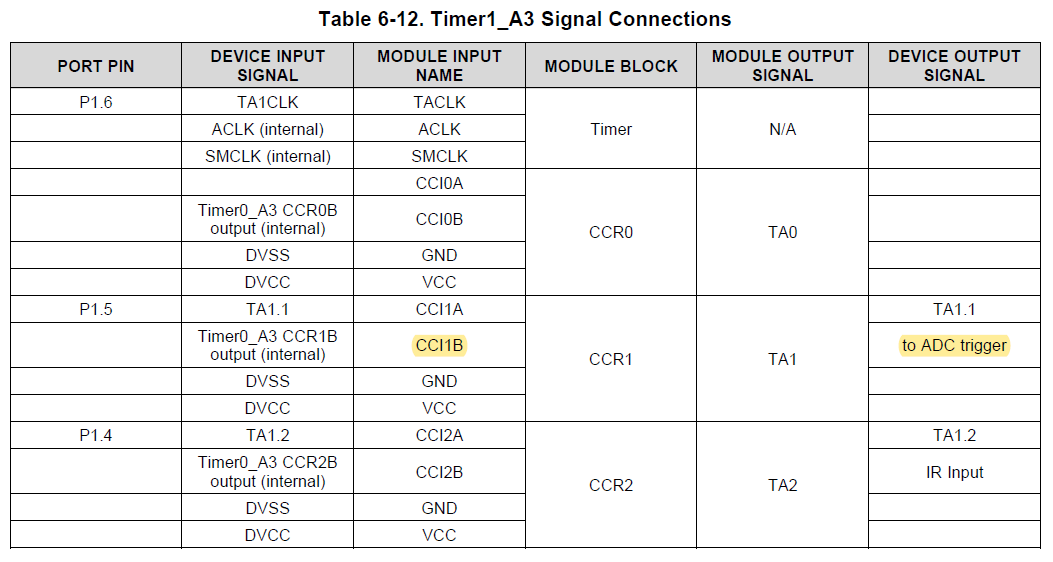
You can also find the TA1.1B (Timer1_A3 CCI1B) is internally connected to the ADC Trigger in Table 6-12 (Timer Signal Connections) of the MSP430FR2433 datasheet.
Configure the voltage reference for the ADC module. In this code example, the internal reference 1.5V is selected as the ADC conversion voltage reference.
 WDTCTL = WDTPW | WDTHOLD;                                   // Stop WDT

 // Configure ADC A0~2 pins
 SYSCFG2 |= ADCPCTL0 | ADCPCTL1 | ADCPCTL2;

 // Disable the GPIO power-on default high-impedance mode to activate
 // previously configured port settings
 PM5CTL0 &= ~LOCKLPM5;

 // Configure ADC
 ADCCTL0 |= ADCSHT_2 | ADCON;                                // 16 ADC clocks, ADC ON
 ADCCTL1 |= ADCSHP | ADCSHS_2 | ADCCONSEQ_3;                 // ADC clock MODCLK, sampling timer, TA1.1B trig., repeat sequence of channels
 ADCCTL2 &= ~ADCRES;                                         // 8-bit conversion results
 ADCMCTL0 |= ADCINCH_2 | ADCSREF_1;                          // Start sample-and-conversion from A2, then A1, A0; Vref is internal 1.5V
 ADCIE |= ADCIE0;                                            // Enable ADC conversion complete interrupt

 // Configure reference
 PMMCTL0_H = PMMPW_H;                                        // Unlock the PMM registers
 PMMCTL2 |= INTREFEN;                                        // Enable internal reference
 __delay_cycles(400);                                        // Delay for reference settling
Configure the Timer1_A3. In this code example, the ADC conversion trigger source is set as Timer1_A3 signal TA1.1B. The period of TA1.1B trigger event should be more than the period taken for ADC sample-and-conversion and ADC interrupt service routine of all the channels. In this example code, the Timer1_A3 output signal TA1.1B is configured as 200us 50% PWM. It will trigger ADC sample-and-conversion every 200us. The 200us is more than the three channels sample-and-conversion time plus the three times ADC subroutine running time.
 // Configure TA1.1B as ADC trigger signal
 // Note: The TA1.1B is configured for 200us 50% PWM, which will trigger ADC
 // sample-and-conversion every 200us. The period of TA1.1B trigger event
 // should be more than the time period taken for ADC sample-and-conversion
 // and ADC interrupt service routine of each channel, which is about 57us in this code
 TA1CCR0 = 200-1;                                            // PWM Period, 200us
 TA1CCTL1 = OUTMOD_7;                                        // CCR1 reset/set
 TA1CCR1 = 100;                                              // CCR1 PWM duty cycle, 50%
 TA1CTL = TASSEL__SMCLK | MC__UP | TACLR;                    // SMCLK, up mode, clear TAR
What description is correct for ADC sample time calculation?
Main loop:
In this code example, the main loop function is simple.
Enable ADC
Trigger the ADC sample-and-conversion start by clearing the Timer1_A3 register TAR to repeatedly start the ADC sample
Enter low power mode LPM0, waiting for ADC interrupt.
while(1)
{
   ADCCTL0 |= ADCENC;                                       // Enable ADC
   TA1CTL |= TACLR;                                         // Clear Timer_A TAR to start the ADC sample
   __bis_SR_register(LPM0_bits | GIE);                      // Enter LPM0 w/ interrupts
   __no_operation();                                        // Only for debug
}
ADC subroutine:
In this code example, the ADC interrupt request will be triggered when each ADC channel conversion is completed.
MCU works in low power mode LPM0. After ADC conversion is completed, the ADC interruption will be triggered.
In the ADC subroutine, the ADC conversion result of channel i is stored in variable
ADC_Result[i]. Please note, the MCU will return to LPM0 mode after the subroutine execution.// ADC interrupt service routine #if defined(__TI_COMPILER_VERSION__) || defined(__IAR_SYSTEMS_ICC__) #pragma vector=ADC_VECTOR __interrupt void ADC_ISR(void) #elif defined(__GNUC__) void __attribute__ ((interrupt(ADC_VECTOR))) ADC_ISR (void) #else #error Compiler not supported! #endif { switch(__even_in_range(ADCIV,ADCIV_ADCIFG)) { case ADCIV_NONE: break; case ADCIV_ADCOVIFG: break; case ADCIV_ADCTOVIFG: break; case ADCIV_ADCHIIFG: break; case ADCIV_ADCLOIFG: break; case ADCIV_ADCINIFG: break; case ADCIV_ADCIFG: ADC_Result[i] = ADCMEM0; if(i == 0) { __no_operation(); // Only for debug i = 2; } else { i--; } break; default: break; } }How many ADC trigger sources are for MSP430FR2433?
Task 2 Code Execution
Connect the PC and LaunchPad with a micro USB cable.
Input the analog voltage signals (may from an adjustable voltage regulator) on the header pin P1.2, P1.1, and P1.0. (Please note the external voltage should be applied on P1.2, P1.1, and P1.0 after the MCU DVCC power-on.)
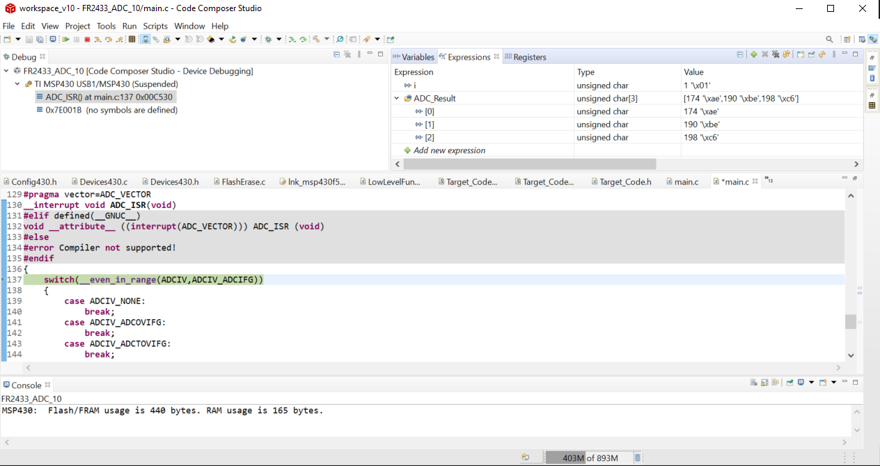
In CCS, build the example code, then program and debug the LaunchPad. Run the code by clicking Run-→Resume button. After a while, click Run→Suspend button. Click the View→Expressions to open the Variables/Expressions/Registers watch window. Input the ADC_Result in the Expression submenu to watch the data value of ADC_Result[0] (for A0), ADC_Result[1] (for A1), and ADC_Result[2] (for A2). The following figure is an example of the capture.
Task 3 – ADC Window Comparator mode to monitor an analog input voltage
Task 3 Example Project Overview
The purpose of this task is to introduce ADC Window Comparator mode functionality on the MSP430. The Window Comparator is used to monitor analog input voltage at low power mode without CPU interaction. The two thresholds ADCHI and ADCLO should be configured with the correct format. When the ADC conversion is completed for the assigned channel, the ADCLO, ADCHI or ADCIN interrupt flags will be triggered. In this example code, the ADC works on Repeat-Single-Channel mode. The ADC input A1 is sampled and ADC conversion every 0.5s with TA1.1B as the trigger signal. Timer TA0 is configured as an interval timer to toggle the P1.0 LED slow, fast, or turn off based on the ADC conversion result for Window Comparator.
- Import the adc_10.c example msp430fr243x_adc10_21.c into CCS from TI Resource Explorer.
MSP430ware→Development Tools→MSP-EXP430FR2433→Peripheral Examples→Register Level→MSP430FR2433→
msp430fr243x_adc10_21.c- Click import in the upper right-hand corner
- Build the code and program it to the LaunchPad.
Task 3 Code Overview
Same as Task #2, let us break down the MSP430 example code into three parts:
- Initialization
- Main loop
- Subroutines
Initialization:
In this code example, the following modules are used: Watchdog, clock system (for CPU and ADC), GPIO, ADC module, voltage reference, TA1, and TA0. These modules need to be configured before the main loop code execution.
The Watchdog module should be disabled to prevent the watchdog timer from triggering a reset while the example code is running.
CPU clock MCLK and SMCLK are default DCODIV ~1MHz. Low-frequency peripheral clock ACLK is configured to crystal oscillator XT1 32768Hz. Please see the detailed initialization code for XT1.
 // Configure XT1 oscillator
 P2SEL0 |= BIT0 | BIT1;                              // P2.0~P2.1: crystal pins

 // Disable the GPIO power-on default high-impedance mode to activate
 // previously configured port settings
 PM5CTL0 &= ~LOCKLPM5;

 CSCTL4 = SELA__XT1CLK;                              // Set ACLK = XT1; MCLK = SMCLK = DCO
 do
 {
    CSCTL7 &= ~(XT1OFFG | DCOFFG);                  // Clear XT1 and DCO fault flag
    SFRIFG1 &= ~OFIFG;
 }while (SFRIFG1 & OFIFG);                           // Test oscillator fault flag
GPIO initialization configures the package pins to assigned functionalities: GPIO output, ADC input. After the GPIO initialization, unlock the GPIO high-impedance mode by reset LOCKLPM5 bit.
Same as Task #1, in this example code, port P1.0 works as GPIO output to blink LED, P1.1 is configured to ADC input function A1. Please note, the input analog signal should be less than 3.6V.
ADC module initialization is to configure ADC related registers: sample-and-hold time and source, simpling signal (SAMPCON) select, ADC clock source, conversion mode, ADC resolution, interrupt enable, ADC sample-and-conversion trigger source.
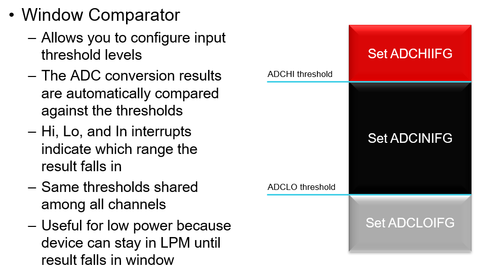
In this example code, ADCCLK is set to ACLK and 16 ADCCLK (MODCLK) cycles setting is selected for sample-and-hold time (see ADCCTL0.ADCSHT), sample-and-hold start signal SAMPCON source is set from sampling timer (see ADCCTL1.ADCSHP), conversion mode is set to Repeat-Single-Channel mode (see ADCCTL1.ADCCONSEQ), 10bit resolution is configured (see ADCCTL2.ADCRES), ADC Window Comparator interrupts are enabled (see ADCIE.ADCHIIE, LOIE, INIE) and ADC sample-and-conversion trigger source is set as TA1.1B (see ADCCTL1.ADCSHS). To enable the ADC Window Comparator, the high threshold (ADCHI) and low threshold (ADCLO) must be set.
 // Configure ADC;
 ADCCTL0 = ADCSHT_2 | ADCON;                         // ADCON
 ADCCTL1 = ADCSHP | ADCSHS_2 | ADCSSEL_1 | ADCCONSEQ_2;          // Rpt single ch; ACLK for ADCCLK; TA1.1 trigger
 ADCCTL2 = ADCRES;                                   // 10-bit conversion results
 ADCMCTL0 = ADCINCH_1 | ADCSREF_1;                   // Vref 1.5v, A1
 ADCHI = High_Threshold;                             // Window Comparator Hi-threshold
 ADCLO = Low_Threshold;                              // Window Comparator Lo-threshold
 ADCIE |= ADCHIIE | ADCLOIE | ADCINIE;               // Enable ADC conversion complete interrupt
Configure the voltage reference for the ADC module. Like Task #1 and #2, in this code example the internal 1.5V reference is selected as the ADC conversion voltage reference.
Configure the Timer0_A3 (TA0) and Timer1_A3 (TA1).
In this code example, the ADC trigger source is set as signal TA1.1B which is configured as 500ms 50% PWM. It will trigger ADC sample-and-conversion every 500ms. TA0 is configured as a simple timer to generate a different frequency for LED blinking by assigning different values for TA0CCR0 in ADC subroutine. The TA0 CCR0 interrupt is enabled for LED toggling in TA0 subroutine.
Both TA1 and TA0 clock source is configured as ACLK.// Configure TA0 period-timer TA0CCTL0 = CCIE; // CCR0 interrupt enabled TA0CTL = TASSEL_1 | TACLR; // ACLK, clear TAR // Configure ADC timer trigger TA1.1 TA1CCR0 = 16384-1; // PWM Period TA1CCR1 = 8192-1; // Duty cycle TA1.1 TA1CCTL1 = OUTMOD_3; // TA1CCR1 set/reset mode TA1CTL = TASSEL_1 | MC_1 | TACLR; // ACLK, up mode ADCCTL0 |= ADCENC; // Enable conversion
Main loop:
In this code example, there is no main loop function. After initialization, the CPU enters low power mode LPM3, waiting for an interrupt from ADC or TA0.
       __bis_SR_register(LPM3_bits | GIE);                 // Enter LPM3 w/ interrupts
       __no_operation();                                   // Only for debugger
What description is correct for ADC low power operation?
ADC subroutine:
After ADC conversion is completed, A1 conversion result is used to compare with ADCHI threshold and ADCLO threshold in ADC module. Based on the result, different interrupt flags (ADCHIIFG, ADCLOIFG, ADCINIFG) will be triggered. Based on the Window Comparator interrupt flags, the ADC subroutine has TA0 settings for different LED toggling rates. When ADCINIFG is triggered, the LED is turned off.
         // ADC interrupt service routine
         #if defined(__TI_COMPILER_VERSION__) || defined(__IAR_SYSTEMS_ICC__)
         #pragma vector=ADC_VECTOR
         __interrupt void ADC_ISR(void)
         #elif defined(__GNUC__)
         void __attribute__ ((interrupt(ADC_VECTOR))) ADC_ISR (void)
         #else
         #error Compiler not supported!
         #endif
         {
            switch(__even_in_range(ADCIV,ADCIV_ADCIFG))
            {
                case ADCIV_NONE:
                    break;
                case ADCIV_ADCOVIFG:
                    break;
                case ADCIV_ADCTOVIFG:
                    break;
                case ADCIV_ADCHIIFG:                            // ADCHI; A1> 1V
                    ADCIFG &= ~ADCHIIFG;                        // Clear interrupt flag
                    TA0CTL &= ~MC_1;                            // Turn off Timer
                    TA0CCR0 = FastToggle_Period;                // Set Timer Period for fast LED toggle
                    TA0CTL |= MC_1;
                    break;
                case ADCIV_ADCLOIFG:                            // ADCLO; A1 < 0.5V
                    ADCIFG &= ~ADCLOIFG;                        // Clear interrupt flag
                    TA0CTL &= ~MC_1;                            // Turn off Timer
                    TA0CCR0 = SlowToggle_Period;               // Set Timer Period for slow LED toggle
                    TA0CTL |= MC_1;
                    break;
                case ADCIV_ADCINIFG:                            // ADCIN; 0.5V < A1 < 1V
                    ADCIFG &= ~ADCINIFG;                        // Clear interrupt flag
                    TA0CTL &= ~MC_1;                            // Turn off Timer
                    P1OUT &= ~BIT0;
                    break;
                case ADCIV_ADCIFG:
                    break;
                default:
                    break;
            }
         }
TA0 subroutine:
In this code example, TA0 subrotine is simple, just to toggle the LED.
       // Timer0 A0 interrupt service routine
       #if defined(__TI_COMPILER_VERSION__) || defined(__IAR_SYSTEMS_ICC__)
       #pragma vector=TIMER0_A0_VECTOR
       __interrupt void TIMER0_A0_ISR(void)
       #elif defined(__GNUC__)
       void __attribute__ ((interrupt(TIMER0_A0_VECTOR))) TIMER0_A0_ISR (void)
       #else
       #error Compiler not supported!
       #endif
       {
         P1OUT ^= BIT0;                                        // Toggle LED P1.0
       }
Task 3 Code Execution
Connect the PC and LaunchPad with a micro USB cable.
Input the analog voltage signal (may from an adjustable voltage regulator) on the header pin P1.1. (Please note the external voltage should be applied on P1.1 after the MCU DVCC power-on. And the voltage on P1.1 should not exceed the specification DVCC+0.3V.)
In CCS, build the example code and program the LaunchPad. Reset the LaunchPad and adjust the voltage on P1.1 (note, the input voltage should be less than 3.6V), and watch the LED blinking status.
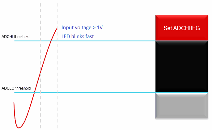
- If the input voltage is greater than 1V, the LED blinks fast.
- If the input voltage is less than 0.5V, the LED blinks slow.
- If the input voltage is between 0.5V and 1V, the LED will be turned off.
Does the board run as expected? If you are running the code without any problem. Congratulations! You are lucky. But you may find the LED will not work as expected. The code may hang up somewhere. Do you know why? ...... Please think about it.
From the following selection, what is the possible root cause for the LED not blinking?
If you debug the code, you will find the code halt at the XT1 initialization. Then check the board, you will find the resistors R2 and R3 are not populated. From the LaunchPad schematic, you will know the crystal Q1 will not work if the R2 and R3 are not populated.
So YES, the root cause is XT1 doesn't work due to a hardware issue. (By default, the MSP430FR2433 LaunchPad will not populate the R2 and R3)
We have two options to fix the issue:
- Remove the R4 and R5. Populate 0-ohm resistors on R2 and R3.
- Comment out the XT1 initialization codes to use REFO as the ACLK source.
Both options can work. In this task, to save time, we can adopt option 2 - comment out the XT1 initialization code as follows.
    // Configure XT1 oscillator
    // P2SEL0 |= BIT0 | BIT1;                              // P2.0~P2.1: crystal pins

    // CSCTL4 = SELA__XT1CLK;                              // Set ACLK = XT1; MCLK = SMCLK = DCO
    // do
    // {
    //     CSCTL7 &= ~(XT1OFFG | DCOFFG);                  // Clear XT1 and DCO fault flag
    //     SFRIFG1 &= ~OFIFG;
    // }while (SFRIFG1 & OFIFG);                           // Test oscillator fault flag
After the issue is resolved, build and program the code into the LaunchPad, then run the code again. You will find the LED blinks as expected when tuning the voltage level on P1.1.
You may want to change the setting of 0.5V and 1V to see different LED blinking behavior. For example, Do you know how to implement the following requirements?
- If the input voltage is greater than 1.2V, the LED blinks fast.
- If the input voltage is less than 0.3V, the LED blinks slow.
- If the input voltage is between 0.3V and 1.2V, the LED will be turned off.
Yes, you are correct! It is to change the high threshold (ADCHI) to 1.2V ADC value and low threshold (ADCLO) to 0.3V ADC value. In the code, it is to change the values for micro definitions High_Threshold and Low_Threshold.
    #define    High_Threshold    818                        //~1.2V
    #define    Low_Threshold     205                        //~0.3V
How to calculate the ADC value:
818 = 1023 * 1.2V / 1.5V.
205 = 1023 * 0.3V / 1.5V.
where 1.5V is the internal Vref voltage, and 1023 is the 10bit ADC full-scale value.
Please change the code, program, and execute the code to see if the LED blinks as expected when tuning the voltage level on P1.1.
If application requests, it is possible to build dynamic window comparator settings for different high threshold (ADCHI) and low threshold (ADCLO) in the ADC subroutine.
You can try it and see the interesting behaviors.
Summary
At the end of this lab, you should now be able to:
- Understand the MSP430 ADC conversion modes, Vref configuration, and low power ADC window comparator operation
- Understand the ADC sample-and-hold time calculation
- Understand the ADC low mode modes operation
- Use different ADC trigger source for different application use cases
This work is licensed under a Creative Commons Attribution-NonCommercial-NoDerivatives 4.0 International License.