Introduction
This lab demonstrates how to use the DMA (Direct Memory Access) module on the MSP-EXP430FR5994. We will demonstrate transferring a 16 word block to the destination address with the DMA on MSP430. This lab uses MSP430Ware register level code examples from MSP430Ware.
The lab has 1 task consisting of the following activities:
- DMA0, Repeated Block to-from RAM, Software Trigger
Prerequisites
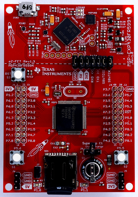
Hardware
The following hardware is required for this lab
Software
Installing the software
NOTE:
The software examples used for this lab should be imported from within the TI Resource Explorer. This can be accessed from the web or locally in CCS by clicking View->Resource Explorer. Prior to importing a Project, you first need to download MSP430Ware in order to be able to import the examples to the CCS IDE. This may be done when CCS was installed or can be done later by clicking the "Download and Install" icon in the top right. Note that installing MSP430Ware for any project will install ALL labs and content, so this only needs to be done once.
Recommended Resources
These training materials provide a baseline introduction to the hardware. This documentation can be referenced for the MSP430 MCU and the launchpad details.
- MSP430FR5994 MCU Datasheet
- MSP430FR58xx, MSP430FR59xx, and MSP430FR6xx Family User's Guide
- MSP430 MCUs Development Guide Book
Overview
Basically DMA is used to transfer data automatically without CPU intervention. This could be to save power or to more efficiently move data while other tasks are being handled by the CPU.
In this lab you will learn about DMA addressing modes, DMA transfer modes and configuring the DMA registers.
Getting Started
Hardware Setup:
Task 1 – DMA0, Repeated Block to-from RAM, Software Trigger
Example Project Overview
The project you will work with shows how to transfer a 16 word block from 1C20h-1C3Fh to 1C40h-1C5Fh using DMA0 in a burst block using software DMAREQ trigger. After each transfer, source, destination and DMA size are reset to initial software setting because DMA transfer mode 5 is used.
Let's build and program the msp430 launchpad with the dma_01.c example to understand what it does.
- Import the dma_01.c example msp430fr599x_dma_01.c into CCS from TI Resource Explorer.
MSP430ware→Development Tools→MSP-EXP430FR5994→Peripheral Examples→Register Level→MSP430FR5994→
msp430fr599x_dma_01.c
- Click import in the upper right hand corner
- Program the launchpad
Code Overview
DMA is a module on our MSP430 MCUs that allows certain integrated modules to access RAM (Random-access Memory) without CPU intervention. With DMA, the CPU first initiates the transfer, then it does other operations while the transfer is in progress, and it finally receives an interrupt from the DMA controller when the operation is done. This feature is useful at any time that the CPU cannot keep up with the rate of data transfer, or when the CPU needs to perform work while waiting for a relatively slow I/O data transfer. Let's find out how to transfer a 16 word block from 1C20h to 1C40h using channel DMA0.
//******************************************************************************
// Main ************************************************************************
// Configure DMA0 to transfer 16 word block from 1C20h to 1C40h. *
//******************************************************************************
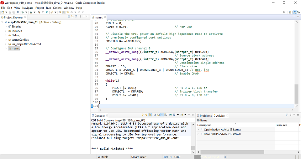
void main {
WDTCTL = WDTPW | WDTHOLD; // Stop WDT
// Configure GPIO
P1OUT = 0;
P1DIR = BIT0; // For LED
// Disable the GPIO power-on default high-impedance mode to activate
// previously configured port settings
PM5CTL0 &= ~LOCKLPM5;
// Configure DMA channel 0
__data20_write_long((uintptr_t) &DMA0SA,(uintptr_t) 0x1C20);
// Source block address
__data20_write_long((uintptr_t) &DMA0DA,(uintptr_t) 0x1C40);
// Destination single address
DMA0SZ = 16; // Block size
DMA0CTL = DMADT_5 | DMASRCINCR_3 | DMADSTINCR_3; // Rpt, inc
DMA0CTL |= DMAEN; // Enable DMA0
while(1)
{
P1OUT |= 0x01; // P1.0 = 1, LED on
DMA0CTL |= DMAREQ; // Trigger block transfer
P1OUT &= ~0x01; // P1.0 = 0, LED off
}
}
main()
First we need to configure the GPIO settings. P1.0 is toggled during DMA transfer only for demonstration purposes. Set P1.0 as LED output pin.
    // Configure GPIO
    P1OUT = 0;
    P1DIR = BIT0;                           // For LED
GPIO setting
Now let's look at the DMA settings. The target of this task is to transfer data from address 1C20h-1C3Fh to address 1C40h-1C5Fh.
DMA Addressing Modes
The DMA controller has four addressing modes. The addressing mode for each DMA channel is independently configurable. For example, channel 0 may transfer between two fixed addresses, while channel 1 transfers between two blocks of addresses. The addressing modes are shown in following figure.
- Fixed address to fixed address
- Fixed address to block of addresses
- Block of addresses to fixed address
Block of addresses to block of addresses
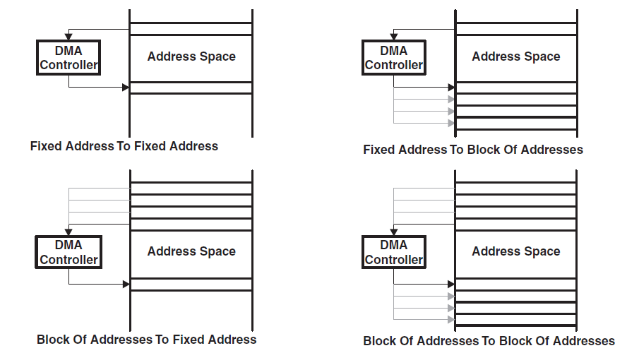
The addressing modes are configured with the DMASRCINCR and DMADSTINCR control bits.
- The DMASRCINCR bits select if the source address is incremented, decremented, or unchanged after each transfer.
- The DMADSTINCR bits select if the destination address is incremented, decremented, or unchanged after each transfer.
Transfers may be byte to byte, word to word, byte to word, or word to byte. When transferring word to byte, only the lower byte of the source word transfers. When transferring byte to word, the upper byte of the destination word is cleared when the transfer occurs.
How to set the DMASRCINCR and DMADSTINCR control bits when we use addressing mode 2 Fixed address to block of addresses?
    // Configure DMA channel 0
    __data20_write_long((uintptr_t) &DMA0SA,(uintptr_t) 0x1C20);
                                            // Source block address
    __data20_write_long((uintptr_t) &DMA0DA,(uintptr_t) 0x1C40);
                                            // Destination single address
    DMA0SZ = 16;                            // Block size
    DMA0CTL = DMADT_5 | DMASRCINCR_3 | DMADSTINCR_3; // Rpt, inc
    DMA0CTL |= DMAEN;                       // Enable DMA0
DMA setting
We set the data source address as 1C20h. Set the data destination address as 1C40h. Set the data length as 16 bytes. And then set the DMASRCINCR and DMADSTINCR as incremented after each transfer.
We also set the DMADT as mode 5. What does that mean?
DMA Transfer Modes
The DMA controller has six transfer modes selected by the DMADT bits as listed in the following table. Each channel is individually configurable for its transfer mode. For example, channel 0 may be configured in single transfer mode, while channel 1 is configured for burst-block transfer mode, and channel 2 operates in repeated block mode. The transfer mode is configured independently from the addressing mode. Any addressing mode can be used with any transfer mode. Two types of data can be transferred selectable by the DMAxCTL DSTBYTE and SRCBYTE fields. The source and destination locations can be either byte or word data. It is also possible to transfer byte to byte, word to word, or any combination.
| DMADT | Transfer Mode | Description |
|---|---|---|
| 000 | Single transfer | Each transfer requires a trigger. DMAEN is automatically cleared when DMAxSZ transfers have been made. |
| 001 | Block transfer | A complete block is transferred with one trigger. DMAEN is automatically cleared at the end of the block transfer. |
| 010,011 | Burst-block transfer | CPU activity is interleaved with a block transfer. DMAEN is automatically cleared at the end of the burst-block transfer. |
| 100 | Repeated single transfer | Each transfer requires a trigger. DMAEN remains enabled. |
| 101 | Repeated block transfer | A complete block is transferred with one trigger. DMAEN remains enabled. |
| 110,111 | Repeated burst-block transfer | CPU activity is interleaved with a block transfer. DMAEN remains enabled. |
Do we need to enable the DMAEN manually every time after transfer completes in repeated block transfer mode?
    while(1)
    {
        P1OUT |= 0x01;                      // P1.0 = 1, LED on
        DMA0CTL |= DMAREQ;                  // Trigger block transfer
        P1OUT &= ~0x01;                     // P1.0 = 0, LED off
    }
configure DMA trigger
After enabling the DMA function, configure software DMA trigger to start transfering data. A transfer is triggered when the DMAREQ bit is set. The DMAREQ bit is automatically reset when the transfer starts.
The following modules can also generate the DMA trigger, halting the CPU immediately and beginning the transfer when a trigger is received:
- DMA
- Timer_A & Timer_B
- eUSCI_Ax & eUSCI_Bx
- ADC12_B
- MPY.
This means you can always find the right trigger source for your application.
Please find more detailed description of the DMA module in the family user's guide.
A Real World Case
Let's discuss a real world case to find out how to set the DMA registers in this application. In this case, you will receive a pack of data from UART RX with UCA0 channel. We want to move the receive data from UCA0RXBUF to RAM start from 0x1C00h to 0x1D00h. We can use the UCA0 receive interrupt as the DMA trigger.
What's the right answer here?
Which addressing mode you would use in this case?
Which transfer mode you would use in this case?
Debug in CCS
Let's build this project and debug it in the CCS. We will check out how does the memory block changed by the code. We first import the project into the CCS workspace and then click Project->Build project button to build the project or you can click this Build button instead. You will find the build finished message in the Console window. It indicates that the project been built successfully. You can also find the error message in the Console window if the build fails.
Connect the MSP-EXP430FR5994 board to your PC with USB cable. Then click Run->Debug button for debugging the project or you can click this Debug button or type in F11 instead.
In the debugging interface, we would like to read out the memory data in the MCU. Click Window->Show View->Memory Browser to show out the Memory Browser window.
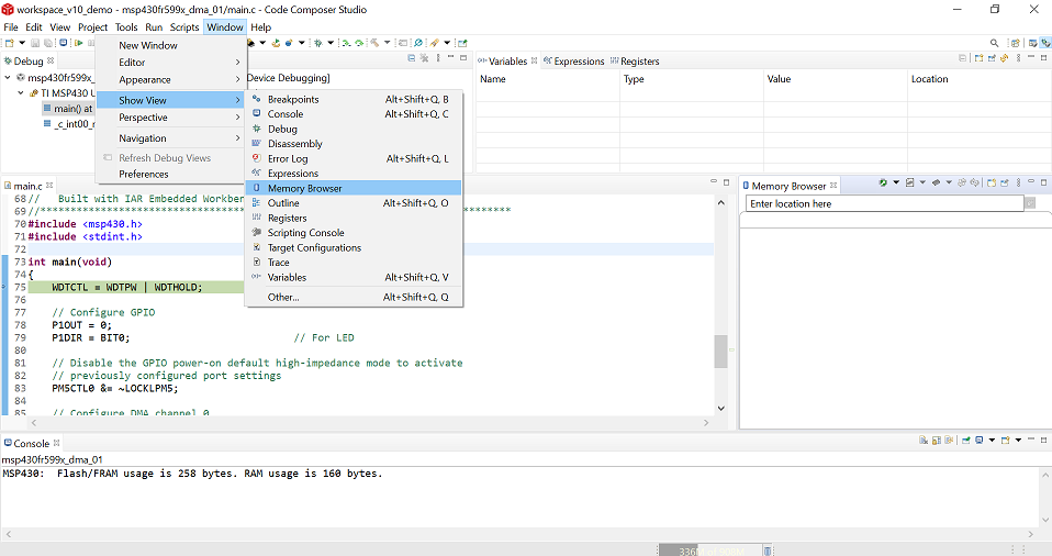
Enter the memory start location you want to observe in the Memory Browser window. In this case, we enter 0x1C20h. Before we run the project, we can fill data 0xFF to 0x1C40h-0x1C5F for better observesion of how the project works. Click Tools->Fill Memory, set the configuration as in the following figure.
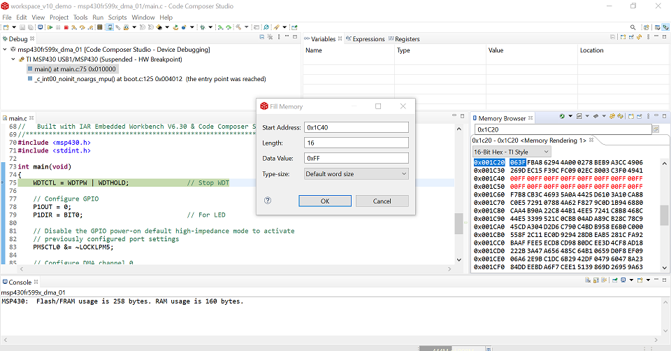
The data in 0x1C40h-0x1C5F has been changed to 0xFF now. Let's run this project now. Click Run->Resume button or click this Resume button or type in F8 instead to start run the project. After running for around half second, click Run->Suspend or click this Suspend button or type in Alt+F8 instead to suspend the debugging to read out the memory.
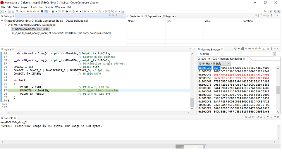
We can find out that the data in 1C20h-1C3Fh has been transferred to 1C40h-1C5Fh. Now, you have learned how to debug a project and view the memory area in CCS.
Quiz
We have learned the basic configuration of the DMA module to transfer data as you need. Now let's look at this code and see if you can predict what it does. Then view the memory area in CCS.
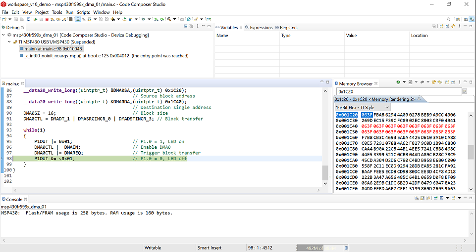
    // Configure DMA channel 0
    __data20_write_long((uintptr_t) &DMA0SA,(uintptr_t) 0x1C20);
                                            // Source block address
    __data20_write_long((uintptr_t) &DMA0DA,(uintptr_t) 0x1C40);
                                            // Destination single address
    DMA0SZ = 16;                            // Block size
    DMA0CTL = DMADT_1 | DMASRCINCR_0 | DMADSTINCR_3; // Block transfer

    while(1)
    {
        P1OUT |= 0x01;                      // P1.0 = 1, LED on
        DMA0CTL |= DMAEN;                   // Enable DMA0
        DMA0CTL |= DMAREQ;                  // Trigger block transfer
        P1OUT &= ~0x01;                     // P1.0 = 0, LED off
    }
DMA quiz
The source address is 1C20h, the destination address is 1C40h. Block size is 16 bytes. We set the DMASRCINCR as unchanged and the DMADSTINCR as incremented. Then we set the DMADT as module 001, the block transfer mode. The means we only transfer the data from 1C20h-1C22h to 1C40h-1C5Fh, the DMA addressing mode is fixed address to block of addresses mode.
Noticed that the DMAEN is cleared by the software after each transferring finished. So in the triggering part, we need to set the DMAEN as enabled in the while loop.
Let's check out the memory result in CCS.
Summary
At the end of this lab, you should now be able to:
- Configure the DMA registers for data transfer
- View the memory area in CCS
This work is licensed under a Creative Commons Attribution-NonCommercial-NoDerivatives 4.0 International License.