Introduction
Welcome to the MSP430 SPI Academy. This lab demonstrates both serial peripheral interface (SPI) controller and peripheral modes of operation using the MSP430FR2433 and its integrated enhanced Universal Serial Communication Interface (eUSCI) module. This lab uses MSP430Ware register-level code examples from MSP430Ware and has three tasks consisting of the following activities:
- Program SPI peripheral MCU
- Program SPI controller MCU and demonstrate controller-to-peripheral basic communication
- Modify SPI controller code to write to a SPI digital-to-analog converter (DAC) on the BOOSTXL-AUDIO BoosterPack
- Modify SPI peripheral code to emulate a SPI DAC
Prerequisites
Before starting this academy, we recommend completing the SPI curriculum in TI's Precision Labs training series to understand SPI fundamentals.
Hardware
The following hardware is required for this lab:
- (2) MSP-EXP430FR2433 LaunchPad
- BOOSTXL-AUDIO BoosterPack Plug-In Module
- Jumper wires
The following tools are not required but are recommended to help with understanding SPI communication better:
- Logic analyzer
- Multimeter
Software
Installing the software
NOTE
The code examples used for this lab should be imported from TI Resource Explorer. They can be accessed from the online Resource Explorer or locally in CCS by clicking View → Resource Explorer. Before importing a project, download MSP430Ware in order to import the examples into the CCS IDE. This may be done when CCS was installed or can be done later by clicking the "Download and Install" icon in the top right. Note that installing MSP430Ware for any project will install ALL labs and content, so this only needs to be done once.
Recommended Resources
These documents can be referenced when using the MSP430 MCU, LaunchPad and BoosterPack.
- MSP430FR2433 MCU Datasheet
- MSP430FR4xx and MSP430FR2xx Family User's Guide
- MSP430FR2433 LaunchPad Development Kit User's Guide
- BOOSTXL-AUDIO Audio BoosterPack Plug-in Module User's Guide
- MSP430 MCUs Development Guide Book
- Solutions to Common eUSCI and USCI Serial Communication Issues on MSP430 MCUs
These training videos provide a basic introduction to the SPI protocol and related hardware.
Overview
This lab introduces SPI communication on MSP430 MCUs by building on material introduced in the SPI Precision Labs training series. The scope of this training academy covers the SPI initialization, operation, and interrupt handling portion of the code examples. Portions of the code examples related to the MCU's clock and general-purpose input-output (GPIO) initialization may be presented for context, but are left up to the reader to investigate separately through other topic-specific TI Academies.
This academy uses two LaunchPads. In Task 1, you will program one LaunchPad with the SPI peripheral code example. In Task 2, you will program the other LaunchPad with the SPI controller code example and demonstrate basic SPI data transmission between the controller and peripheral devices. In Task 3, you will have the opportunity to use your SPI knowledge to modify the SPI controller code example to write data to the 14-bit DAC8311 installed on the BOOSTXL-AUDIO BoosterPack module. In Task 4 you will be challenged to take your SPI knowledge one step further by modifying the SPI peripheral code example to emulate the behavior of a SPI device, such as the DAC8311.
Getting Started
Hardware Setup
- (2) MSP-EXP430FR2433 LaunchPad
- (7) Jumper wires
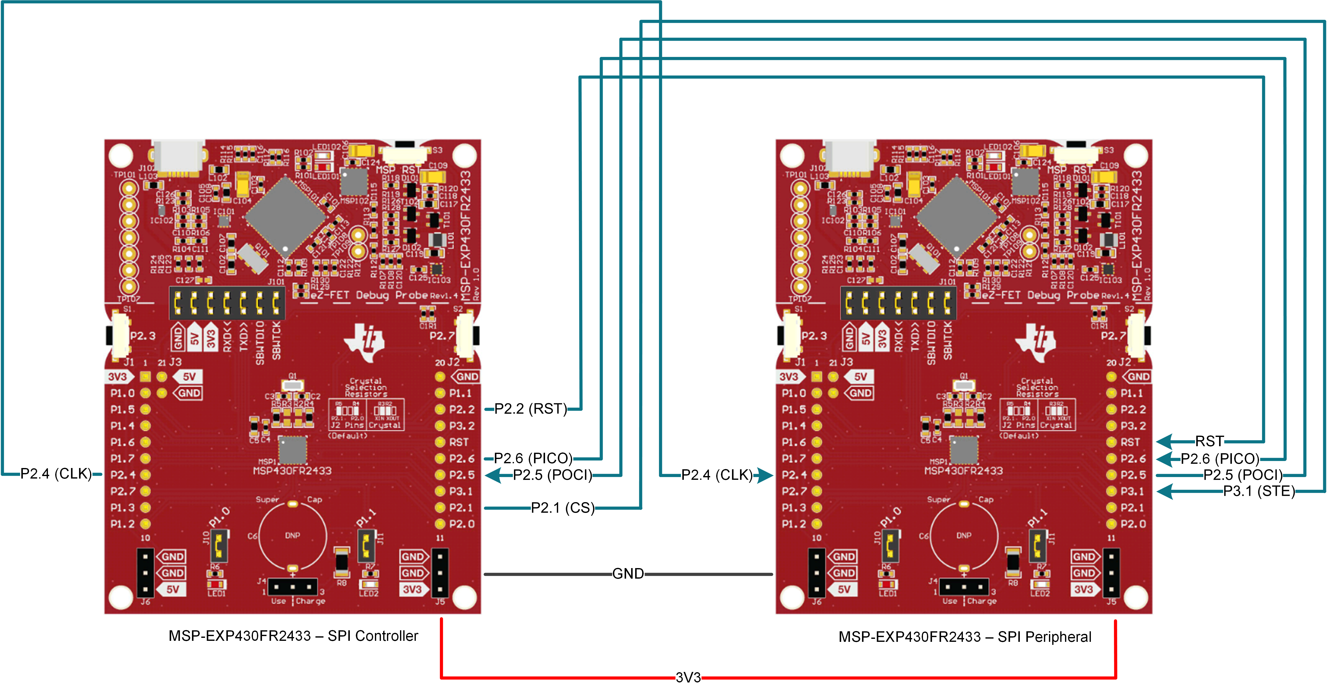
To connect the MSP430FR2433 LaunchPads for SPI communication:
- Choose one of the LaunchPads to be the SPI controller device and the other LaunchPad to be the SPI peripheral device.
- Using jumper wires, make the connections between the two LaunchPads.
Note that the RST jumper wire is optional.
IMPORTANT NOTE
Let's assume you've connected the LaunchPads together. Before programming or debugging one of the LaunchPads, make sure you remove ALL jumpers from the Isolation Jumper Block (J101) on the other LaunchPad. This precaution avoids power supply conflicts and prevents the onboard debugger on the other LaunchPad from getting backpowered, which may put the target MSP430 into reset or an unknown state.
Also, if you encounter
Error connecting to the target: Unknown devicein CCS when programming or debugging a LaunchPad, remove the RST jumper wire.
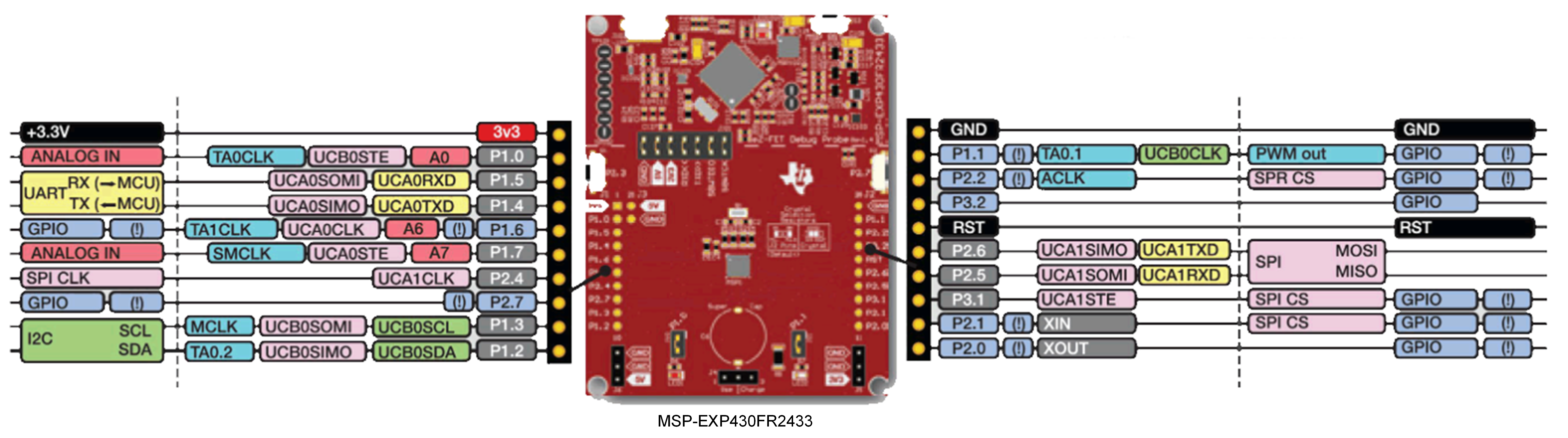
LaunchPad Connections
LaunchPad Pinout
Task 1. Import Example Project and Program SPI Peripheral Device
Task 1. Example Project Overview
The purpose of Task 1 is to select one of the MSP430FR2433 LaunchPads and program it with the SPI peripheral code example shown below. For this task, no modification of the code example is required.
- Import the SPI peripheral example msp430fr243x_eusci_spi_standard_slave.c into CCS from TI Resource Explorer.
- Software → MSP430Ware → Development Tools → MSP-EXP430FR2433 → Peripheral Examples → Register Level → MSP430FR2433 →
msp430fr243x_eusci_spi_standard_slave.c 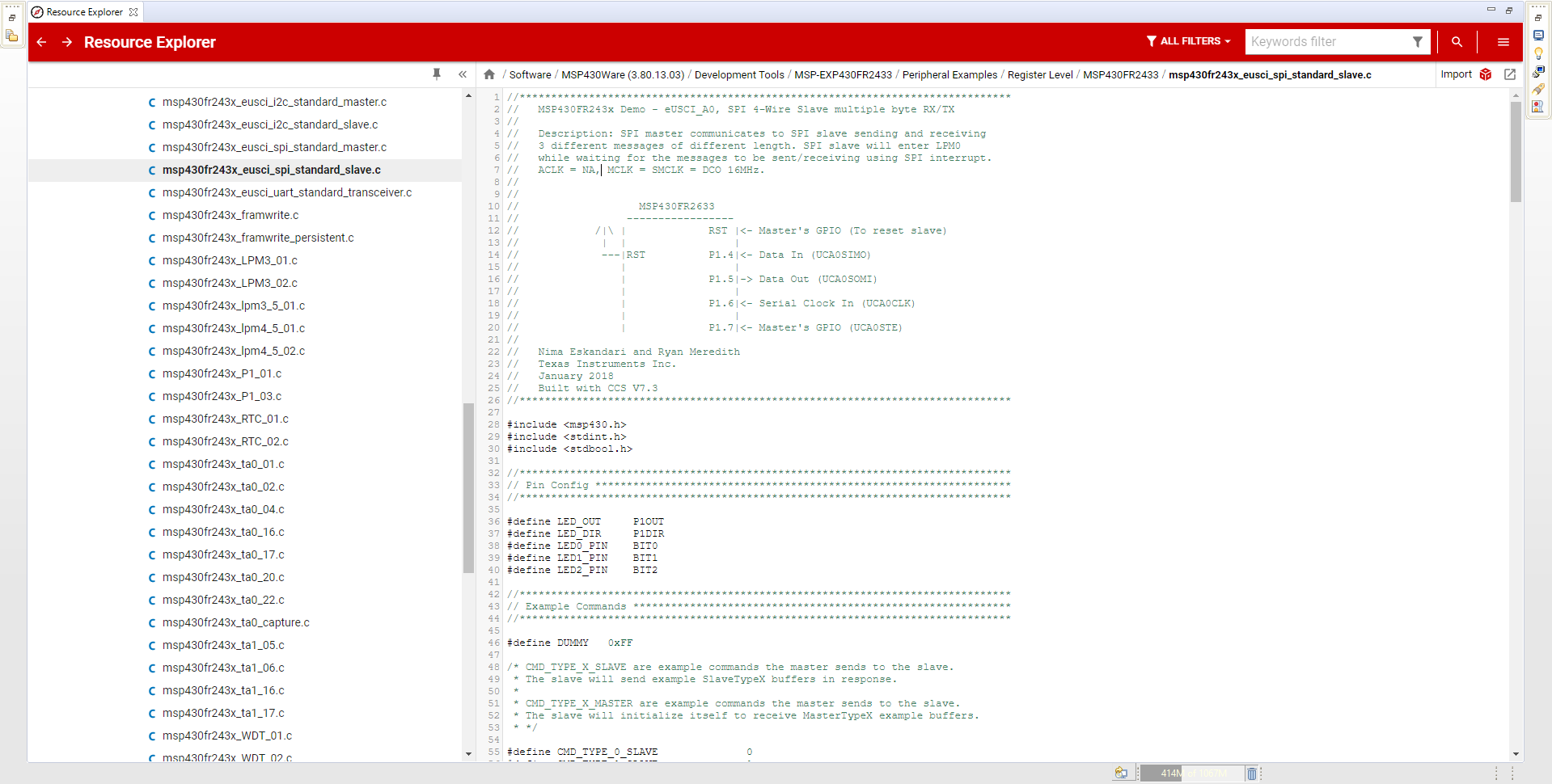
- Click Import in the upper right-hand corner
- Software → MSP430Ware → Development Tools → MSP-EXP430FR2433 → Peripheral Examples → Register Level → MSP430FR2433 →
- Program the LaunchPad and designate it as your SPI Peripheral LaunchPad for future tasks.
Task 1. Software Overview
Starting in the main() function, the typical initialization tasks, such as disabling the watchdog timer, configuring the system clocks, initializing the GPIO pins and configuring the SPI module in peripheral mode, are performed.
Then, the code places the MSP430 into a low-power mode where the CPU will remain halted until a character is received from the SPI controller.
When a SPI character is received, a SPI interrupt is generated, waking the CPU from its low-power mode.
The code will then process the received character in the SPI interrupt service routine (ISR).
After the processing has completed, the code exits from the ISR, and the CPU returns to its low-power mode.
    int main(void)
    {
        // Stop watchdog timer
        WDTCTL = WDTPW | WDTHOLD;

        // Initialize device
        initClockTo16MHz();
        initGPIO();
        initSPI();

        // Enter LPM0 w/interrupts enabled
        __bis_SR_register(LPM0_bits + GIE);
        __no_operation();
        return 0;
    }
main() Function
Let's take a look at the SPI initialization steps. Before modifying any registers, always put the eUSCI module into its reset state, UCA1CTLW0 = UCSWRST.
Next, configure the eUSCI module as an 8-bit synchronous SPI peripheral in 4-pin mode with the most significant byte (MSB) transmitted/received first.
We must also ensure that the SPI clock polarity and phase match or else the SPI peripheral won't be able to communicate with the SPI controller.
In this code example, the selected clock polarity ensures that the inactive state is high. All of these settings are configured by UCA1CTLW0 |= UCCKPL | UCMSB | UCSYNC | UCMODE_2.
That's it! The eUSCI module can then be released from its reset state, UCA1CTLW0 &= ~UCSWRST.
The last things to configure are the interrupts. SPI interrupts are used to notify the CPU when certain SPI events have occurred during a SPI transaction.
In this code example, we want to know when data has been received and loaded into the receive buffer. To capture this event, we set the corresponding interrupt enable bit, UCA1IE |= UCRXIE.
    void initSPI()
    {
        // Clock polarity select: inactive state is high, MSB first
        // 8-bit data, Synchronous, Slave mode, 4-pin SPI
        UCA1CTLW0 = UCSWRST;                    // **Put eUSCI module in reset**
        UCA1CTLW0 |= UCCKPL | UCMSB | UCSYNC |
                    UCMODE_2;
        UCA1CTLW0 &= ~UCSWRST;                  // **Initialize eUSCI module**
        UCA1IE |= UCRXIE;                       // Enable eUSCI0 RX interrupt
    }
SPI Peripheral Initialization
Next, let's take a look at the commands and the state machine that processes the commands and data.
For the transactions between the SPI controller and SPI peripheral devices to work correctly, both devices must agree on how the data is represented. In this case, the command definitions shown below are used in both the SPI controller and peripheral code examples.
There are six example commands: CMD_TYPE_X_MASTER and CMD_TYPE_X_SLAVE. The three CMD_TYPE_X_MASTER commands represent data that the SPI controller will write to the SPI peripheral's corresponding receive buffers. The three CMD_TYPE_X_SLAVE commands represent data that the SPI controller will read from the SPI peripheral's corresponding transmit buffers. Notice that there is a different command based on the size or amount of data in the transaction. Note that these commands are completely arbitrary, but one possible use for the three CMD_TYPE_X_SLAVE commands could be used to represent the SPI peripheral's information such as an ID, current time, location or other information. For this example, the CMD_TYPE_X_MASTER and CMD_TYPE_X_SLAVE commands have been assigned arbitrary values.
    #define DUMMY                   0xFF

    /* CMD_TYPE_X_SLAVE are example commands the master sends to the slave.
    * The slave will send example SlaveTypeX buffers in response.
    *
    * CMD_TYPE_X_MASTER are example commands the master sends to the slave.
    * The slave will initialize itself to receive MasterTypeX example buffers.
    * */

    #define CMD_TYPE_0_SLAVE        0
    #define CMD_TYPE_1_SLAVE        1
    #define CMD_TYPE_2_SLAVE        2

    #define CMD_TYPE_0_MASTER       3
    #define CMD_TYPE_1_MASTER       4
    #define CMD_TYPE_2_MASTER       5

    #define TYPE_0_LENGTH           1
    #define TYPE_1_LENGTH           2
    #define TYPE_2_LENGTH           6
SPI Example Command Definitions
There are two types of arrays used as buffers: MasterTypeX[] and SlaveTypeX[]. A MasterTypeX[] array is a receive buffer and a SlaveTypeX[] array is a transmit buffer in the context of SPI peripheral device. The size of each array is defined by the corresponding TYPE_X_LENGTH.
Here is an example of how they are used. Assume the SPI controller wants to write two bytes to the SPI peripheral device. The SPI controller sends the CMD_TYPE_1_MASTER command byte, followed by two bytes of data (as defined by TYPE_1_LENGTH).
The SPI peripheral decodes the command, prepares to receive the next two bytes and store them in its corresponding MasterType1[] receive buffer. Likewise, if the SPI controller wants to read six bytes from the SPI peripheral, it sends the CMD_TYPE_2_SLAVE command byte. The SPI peripheral will prepare its corresponding transmit buffer with six bytes (as defined by the TYPE_2_LENGTH).
When the SPI controller performs the read operation, the six bytes are transmitted from the corresponding SlaveType2[] transmit buffers.
    /* MasterTypeX are example buffers initialized in the master, they will be
    * sent by the master to the slave.
    * SlaveTypeX are example buffers initialized in the slave, they will be
    * sent by the slave to the master.
    * */

    uint8_t MasterType2 [TYPE_2_LENGTH] = {0};
    uint8_t MasterType1 [TYPE_1_LENGTH] = {0, 0};
    uint8_t MasterType0 [TYPE_0_LENGTH] = {0};

    uint8_t SlaveType2 [TYPE_2_LENGTH]  = {'A', 'B', 'C', 'D', '1', '2'};
    uint8_t SlaveType1 [TYPE_1_LENGTH]  = {0x15, 0x16};
    uint8_t SlaveType0 [TYPE_0_LENGTH]  = {12};
SPI Peripheral Example Buffers
Here is the initial command processing function.
    void SPI_Slave_ProcessCMD(uint8_t cmd)
    {
        ReceiveIndex = 0;
        TransmitIndex = 0;
        RXByteCtr = 0;
        TXByteCtr = 0;

        switch (cmd)
        {
            // Send slave device ID (this device's ID)
            case (CMD_TYPE_0_SLAVE):
                SlaveMode = TX_DATA_MODE;
                TXByteCtr = TYPE_0_LENGTH;
                // Fill out the TransmitBuffer
                CopyArray(SlaveType0, TransmitBuffer, TYPE_0_LENGTH);
                // Send next byte
                SendUCA1Data(TransmitBuffer[TransmitIndex++]);
                TXByteCtr--;
                break;

            // Send slave device time (this device's time)
            case (CMD_TYPE_1_SLAVE):
                SlaveMode = TX_DATA_MODE;
                TXByteCtr = TYPE_1_LENGTH;
                // Fill out the TransmitBuffer
                CopyArray(SlaveType1, TransmitBuffer, TYPE_1_LENGTH);
                // Send next byte
                SendUCA1Data(TransmitBuffer[TransmitIndex++]);
                TXByteCtr--;
                break;

            // Send slave device location (this device's location)
            case (CMD_TYPE_2_SLAVE):
                SlaveMode = TX_DATA_MODE;
                TXByteCtr = TYPE_2_LENGTH;
                // Fill out the TransmitBuffer
                CopyArray(SlaveType2, TransmitBuffer, TYPE_2_LENGTH);
                // Send next byte
                SendUCA1Data(TransmitBuffer[TransmitIndex++]);
                TXByteCtr--;
                break;

            case (CMD_TYPE_0_MASTER):
                SlaveMode = RX_DATA_MODE;
                RXByteCtr = TYPE_0_LENGTH;
                break;

            case (CMD_TYPE_1_MASTER):
                SlaveMode = RX_DATA_MODE;
                RXByteCtr = TYPE_1_LENGTH;
                break;

            case (CMD_TYPE_2_MASTER):
                SlaveMode = RX_DATA_MODE;
                RXByteCtr = TYPE_2_LENGTH;
                break;

            default:
                __no_operation();
                break;
        }
    }
SPI Peripheral Initial Command Processing Function
Here is the final command processing function.
    void SPI_Slave_TransactionDone(uint8_t cmd)
    {
        switch (cmd)
        {
            // Slave device ID was sent (this device's ID)
            case (CMD_TYPE_0_SLAVE):
                break;

            // Slave device time was sent (this device's time)
            case (CMD_TYPE_1_SLAVE):
                break;

            // Slave device location was sent (this device's location)
            case (CMD_TYPE_2_SLAVE):
                break;

            case (CMD_TYPE_0_MASTER):
                CopyArray(ReceiveBuffer, MasterType0, TYPE_0_LENGTH);
                break;

            case (CMD_TYPE_1_MASTER):
                CopyArray(ReceiveBuffer, MasterType1, TYPE_1_LENGTH);
                break;

            case (CMD_TYPE_2_MASTER):
                CopyArray(ReceiveBuffer, MasterType2, TYPE_2_LENGTH);
                break;

            default:
                __no_operation();
                break;
        }
    }
SPI Peripheral Final Command Processing Function
The ISR is set up to work as a state machine, controlling the flow of the code based on the state of the SPI transactions.
    #if defined(__TI_COMPILER_VERSION__) || defined(__IAR_SYSTEMS_ICC__)
    #pragma vector=USCI_A1_VECTOR
    __interrupt void USCI_A1_ISR(void)
    #elif defined(__GNUC__)
    void __attribute__ ((interrupt(USCI_A1_VECTOR))) USCI_A1_ISR (void)
    #else
    #error Compiler not supported!
    #endif
    {
        uint8_t uca1_rx_val = 0;
        switch(__even_in_range(UCA1IV, USCI_SPI_UCTXIFG))
        {
            case USCI_NONE: break;
            case USCI_SPI_UCRXIFG:
                uca1_rx_val = UCA1RXBUF;
                UCA1IFG &= ~UCRXIFG;
                switch (SlaveMode)
                {
                    case (RX_REG_ADDRESS_MODE):
                        ReceiveRegAddr = uca1_rx_val;
                        SPI_Slave_ProcessCMD(ReceiveRegAddr);
                        break;
                    case (RX_DATA_MODE):
                        // Store received byte
                        ReceiveBuffer[ReceiveIndex++] = uca1_rx_val;
                        RXByteCtr--;
                        if (RXByteCtr == 0)
                        {
                            // Done with reception
                            SlaveMode = RX_REG_ADDRESS_MODE;
                            SPI_Slave_TransactionDone(ReceiveRegAddr);
                        }
                        break;
                    case (TX_DATA_MODE):
                        if (TXByteCtr > 0)
                        {
                            // Send additional byte
                            SendUCA1Data(TransmitBuffer[TransmitIndex++]);
                            TXByteCtr--;
                        }
                        if (TXByteCtr == 0)
                        {
                            // Done with transmission
                            SlaveMode = RX_REG_ADDRESS_MODE;
                            SPI_Slave_TransactionDone(ReceiveRegAddr);
                        }
                        break;
                    default:
                        __no_operation();
                        break;
                    }
                break;
            case USCI_SPI_UCTXIFG:
                break;
            default: break;
        }
    }
State Machine Inside SPI ISR
Task 2. Import Example Project and Program SPI Controller Device
Task 2. Example Project Overview
The purpose of this task is to introduce SPI controller functionality on the MSP430 and describe how to communicate with another MSP430 running the SPI peripheral example from Task 1. For this task, no modification to the code example is required.
- Import the SPI controller example msp430fr243x_eusci_spi_standard_master.c into CCS from TI Resource Explorer.
- Software → MSP430Ware → Development Tools → MSP-EXP430FR2433 → Peripheral Examples → Register Level → MSP430FR2433 →
msp430fr243x_eusci_spi_standard_master.c 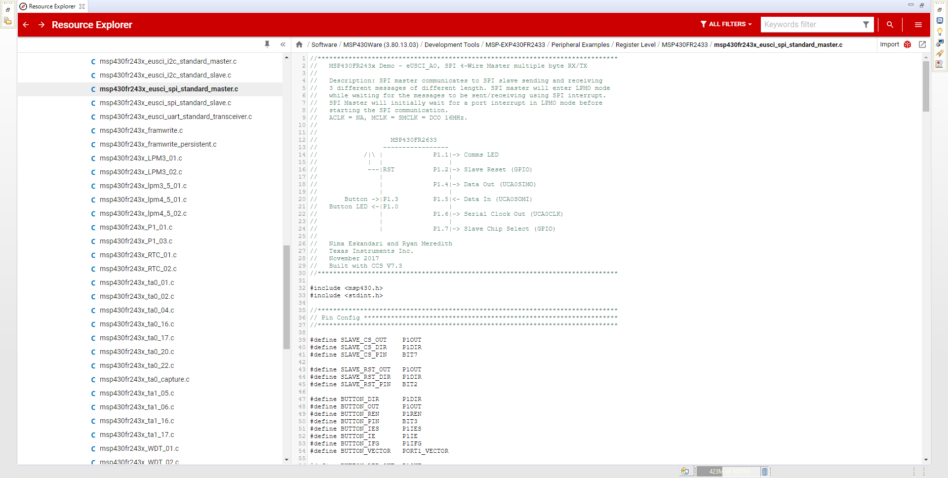
- Click Import in the upper right-hand corner
- Software → MSP430Ware → Development Tools → MSP-EXP430FR2433 → Peripheral Examples → Register Level → MSP430FR2433 →
- Program the second LaunchPad and designate it as your SPI Controller LaunchPad for future tasks.
Task 2. Software Overview
Starting in the main() function, similar to the SPI peripheral code example, the typical initialization tasks, such as disabling the watchdog timer, configuring the system clocks, initializing the GPIO pins and configuring the SPI module in controller mode, are performed. Next, the SPI controller resets the SPI peripheral to ensure it has been initialized properly. The code places the MSP430 into a low-power mode where the CPU will remain halted until a high-to-low transition is detected on a specific GPIO. This transition generates a Port interrupt, waking the CPU from its low-power mode. The SPI controller code will then demonstrate all six example commands. The first three CMD_TYPE_X_SLAVE commands perform read operations, requesting different lengths of data from the SPI peripheral. The last three CMD_TYPE_X_MASTER commands perform write operations, sending different lengths of data to the SPI peripheral. After the transactions finish, the code places the MSP430 back into a low-power mode.
    int main(void)
    {
        // Stop watchdog timer
        WDTCTL = WDTPW | WDTHOLD;

        // Initialize device
        initClockTo16MHz();
        initGPIO();
        initSPI();

        while(1)
        {
            // Reset slave after initializing eUSCI pins
            COMMS_LED_OUT &= ~COMMS_LED_PIN;        // Turn off comms LED
            SLAVE_RST_OUT &= ~SLAVE_RST_PIN;        // Reset slave
            __delay_cycles(100000);                 // Wait
            SLAVE_RST_OUT |= SLAVE_RST_PIN;         // Release slave
            __delay_cycles(100000);                 // Wait for slave to initialize
            COMMS_LED_OUT |= COMMS_LED_PIN;         // Turn on comms LED

            // Enter LPM0 w/interrupts enabled
            __bis_SR_register(LPM0_bits + GIE);

            // CPU wakes up on button press, starts communication
            SPI_Master_ReadReg(CMD_TYPE_2_SLAVE, TYPE_2_LENGTH);
            CopyArray(ReceiveBuffer, SlaveType2, TYPE_2_LENGTH);

            SPI_Master_ReadReg(CMD_TYPE_1_SLAVE, TYPE_1_LENGTH);
            CopyArray(ReceiveBuffer, SlaveType1, TYPE_1_LENGTH);

            SPI_Master_ReadReg(CMD_TYPE_0_SLAVE, TYPE_0_LENGTH);
            CopyArray(ReceiveBuffer, SlaveType0, TYPE_0_LENGTH);

            SPI_Master_WriteReg(CMD_TYPE_2_MASTER, MasterType2, TYPE_2_LENGTH);
            SPI_Master_WriteReg(CMD_TYPE_1_MASTER, MasterType1, TYPE_1_LENGTH);
            SPI_Master_WriteReg(CMD_TYPE_0_MASTER, MasterType0, TYPE_0_LENGTH);

            // Re-enable button to repeat transfer
            BUTTON_IE  |= BUTTON_PIN;               // Button interrupt enabled
            BUTTON_LED_OUT &= ~BUTTON_LED_PIN;      // Turn off button LED
        }
    }
main() Function
Let's take a look at the SPI initialization steps. Before modifying any registers, always put the eUSCI module into its reset state, UCA1CTLW0 = UCSWRST.
Next, configure the eUSCI module as an 8-bit synchronous SPI controller in 3-pin mode with the most significant byte (MSB) transmitted/received first, using SMCLK for the BRCLK source.
We must also ensure that the SPI clock polarity and phase match or else the SPI controller won't be able to communicate with the SPI peripheral.
In this code example, the selected clock polarity ensures that the inactive state is high. All of these settings are configured by UCA1CTLW0 |= UCCKPL | UCMSB | UCSYNC | UCMST | UCSSEL__SMCLK.
SMCLK is sourced from the 16MHz digitally controlled oscillator (DCO), so it must be divided down using UCA1BRW = 80 to meet our 100kHz SPI clock requirement, since we are using jumper wires.
That's it! The eUSCI module can then be released from its reset state, UCA1CTLW0 &= ~UCSWRST.
The last things to configure are the interrupts. SPI interrupts are used to notify the CPU when certain SPI events have occurred during a SPI transaction.
In this code example, we want to know when data has been received and loaded into the receive buffer. To capture this event, we set the corresponding interrupt enable bit, UCA1IE |= UCRXIE.
    void initSPI()
    {
        // Clock polarity select: inactive state is high, MSB first
        // 8-bit data, Synchronous, Master mode, 3-pin SPI, BRCLK source: SMCLK
        UCA1CTLW0 = UCSWRST;                    // **Put eUSCI module in reset**
        UCA1CTLW0 |= UCCKPL | UCMSB | UCSYNC |
                    UCMST | UCSSEL__SMCLK;
        UCA1BRW = 80;                           // BRCLK / UCBRx = UCxCLK   [JE] Update this
                                                // 8MHz  / 80    = 100kHz
        UCA1CTLW0 &= ~UCSWRST;                  // **Initialize eUSCI module**
        UCA1IE |= UCRXIE;                       // Enable eUSCI0 RX interrupt
    }
SPI Controller Initialization
Next, let's take a look at the commands.
For the transactions between the SPI controller and SPI peripheral devices to work correctly, both devices must agree on how the data is represented. In this case, the command definitions shown below are used in both the SPI controller and peripheral code examples.
There are six example commands: CMD_TYPE_X_MASTER and CMD_TYPE_X_SLAVE. The three CMD_TYPE_X_MASTER commands represent data that the SPI controller will write to the SPI peripheral's corresponding receive buffers. The three CMD_TYPE_X_SLAVE commands represent data that the SPI controller will read from the SPI peripheral's corresponding transmit buffers. Notice that there is a different command based on the size or amount of data in the transaction. Note that these commands are completely arbitrary, but one possible use for the three CMD_TYPE_X_SLAVE commands could be used to represent the SPI peripheral's information such as an ID, current time, location or other information. For this example, the CMD_TYPE_X_MASTER and CMD_TYPE_X_SLAVE commands have been assigned arbitrary values.
    #define DUMMY                   0xFF

    /* CMD_TYPE_X_SLAVE are example commands the master sends to the slave.
    * The slave will send example SlaveTypeX buffers in response.
    *
    * CMD_TYPE_X_MASTER are example commands the master sends to the slave.
    * The slave will initialize itself to receive MasterTypeX example buffers.
    * */

    #define CMD_TYPE_0_SLAVE        0
    #define CMD_TYPE_1_SLAVE        1
    #define CMD_TYPE_2_SLAVE        2

    #define CMD_TYPE_0_MASTER       3
    #define CMD_TYPE_1_MASTER       4
    #define CMD_TYPE_2_MASTER       5

    #define TYPE_0_LENGTH           1
    #define TYPE_1_LENGTH           2
    #define TYPE_2_LENGTH           6
SPI Example Command Definitions
There are two types of arrays used as buffers: MasterTypeX[] and SlaveTypeX[]. A MasterTypeX[] array is a transmit buffer and a SlaveTypeX[] array is a receive buffer in the context of SPI controller device. The size of each array is defined by the corresponding TYPE_X_LENGTH.
    /* MasterTypeX are example buffers initialized in the master, they will be
    * sent by the master to the slave.
    * SlaveTypeX are example buffers initialized in the slave, they will be
    * sent by the slave to the master.
    * */

    uint8_t MasterType0 [TYPE_0_LENGTH] = {0x11};
    uint8_t MasterType1 [TYPE_1_LENGTH] = {8, 9};
    uint8_t MasterType2 [TYPE_2_LENGTH] = {'F', '4', '1', '9', '2', 'B'};

    uint8_t SlaveType2 [TYPE_2_LENGTH]  = {0};
    uint8_t SlaveType1 [TYPE_1_LENGTH]  = {0};
    uint8_t SlaveType0 [TYPE_0_LENGTH]  = {0};
SPI Controller Example Buffers
The SPI controller's write register function is shown below and is used to write data to the SPI peripheral device. This function accepts three arguments.
The reg_addr argument is the register address, or command, which is defined above. However, if the SPI peripheral device is a sensor, this value would come from the sensor's datasheet.
The *reg_data argument is the data to write, and the count argument is the length of the data.
    SPI_Mode SPI_Master_WriteReg(uint8_t reg_addr, uint8_t *reg_data, uint8_t count)
    {
        MasterMode = TX_REG_ADDRESS_MODE;
        TransmitRegAddr = reg_addr;

        // Copy register data to TransmitBuffer
        CopyArray(reg_data, TransmitBuffer, count);

        TXByteCtr = count;
        RXByteCtr = 0;
        ReceiveIndex = 0;
        TransmitIndex = 0;

        SLAVE_CS_OUT &= ~(SLAVE_CS_PIN);
        SendUCA1Data(TransmitRegAddr);

        __bis_SR_register(CPUOFF + GIE);        // Enter LPM0 w/interrupts enabled

        SLAVE_CS_OUT |= SLAVE_CS_PIN;
        return MasterMode;
    }
SPI Controller Write Register Function
The SPI controller's read register function is shown below and is used to read data from the SPI peripheral device. This function accepts two arguments.
The reg_addr argument is the register address, or command, which is defined above. Again, if the SPI peripheral device is a sensor, this value would come from the sensor's datasheet.
The count argument is the length of the data. After each data byte has been read, it is copied into the ReceiveBuffer[] array.
    SPI_Mode SPI_Master_ReadReg(uint8_t reg_addr, uint8_t count)
    {
        MasterMode = TX_REG_ADDRESS_MODE;
        TransmitRegAddr = reg_addr;
        RXByteCtr = count;
        TXByteCtr = 0;
        ReceiveIndex = 0;
        TransmitIndex = 0;

        SLAVE_CS_OUT &= ~(SLAVE_CS_PIN);
        SendUCA1Data(TransmitRegAddr);

        __bis_SR_register(CPUOFF + GIE);        // Enter LPM0 w/interrupts enabled

        SLAVE_CS_OUT |= SLAVE_CS_PIN;
        return MasterMode;
    }
SPI Controller Read Register Function
The switch statement in the SPI controller's ISR functions as a state machine.
    #if defined(__TI_COMPILER_VERSION__) || defined(__IAR_SYSTEMS_ICC__)
    #pragma vector=USCI_A1_VECTOR
    __interrupt void USCI_A1_ISR(void)
    #elif defined(__GNUC__)
    void __attribute__ ((interrupt(USCI_A1_VECTOR))) USCI_A1_ISR (void)
    #else
    #error Compiler not supported!
    #endif
    {
        uint8_t uca1_rx_val = 0;
        switch(__even_in_range(UCA1IV, USCI_SPI_UCTXIFG))
        {
            case USCI_NONE: break;
            case USCI_SPI_UCRXIFG:
                uca1_rx_val = UCA1RXBUF;
                UCA1IFG &= ~UCRXIFG;
                switch (MasterMode)
                {
                    case TX_REG_ADDRESS_MODE:
                        if (RXByteCtr)
                        {
                            // Need to start receiving now
                            MasterMode = RX_DATA_MODE;

                            // Send dummy byte to start
                            __delay_cycles(5000);
                            SendUCA1Data(DUMMY);
                        }
                        else
                        {
                            // Continue to transmission
                            MasterMode = TX_DATA_MODE;

                            // Send first byte
                            SendUCA1Data(TransmitBuffer[TransmitIndex++]);
                            TXByteCtr--;
                        }
                        break;

                    case TX_DATA_MODE:
                        if (TXByteCtr)
                        {
                            // Send additional byte
                            SendUCA1Data(TransmitBuffer[TransmitIndex++]);
                            TXByteCtr--;
                        }
                        else
                        {
                            // Done with transmission
                            MasterMode = IDLE_MODE;
                            __bic_SR_register_on_exit(CPUOFF);  // Exit LPM0
                        }
                        break;

                    case RX_DATA_MODE:
                        if (RXByteCtr)
                        {
                            // Store received byte
                            ReceiveBuffer[ReceiveIndex++] = uca1_rx_val;
                            RXByteCtr--;
                        }
                        if (RXByteCtr == 0)
                        {
                            // Done with reception
                            MasterMode = IDLE_MODE;
                            __bic_SR_register_on_exit(CPUOFF);  // Exit LPM0
                        }
                        else
                        {
                            // Send dummy byte to receive next byte
                            SendUCA1Data(DUMMY);
                        }
                        break;

                    default:
                        __no_operation();
                        break;
                }
                __delay_cycles(1000);
                break;
            case USCI_SPI_UCTXIFG:
                break;
            default: break;
        }
    }
State Machine Inside SPI ISR
Task 2. Logic Analyzer Captures
After programming both devices, reset the SPI Peripheral LaunchPad to initialize it properly before starting the communication by briefly pressing the RESET button (S3) at the top of the LaunchPad near the USB connector. Then, repeat this step on the SPI Controller LaunchPad.
The next capture shows the first read operation performed by the SPI controller.
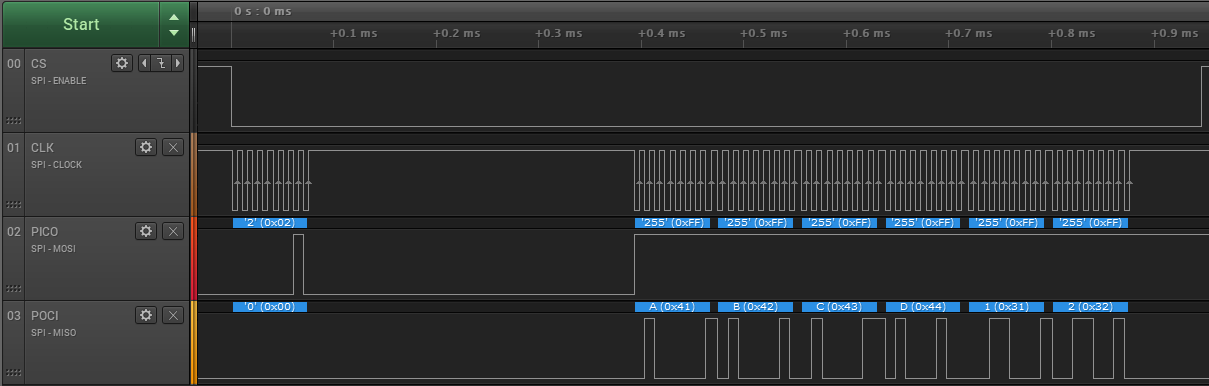
The capture shown below is the first write operation performed by the SPI controller.
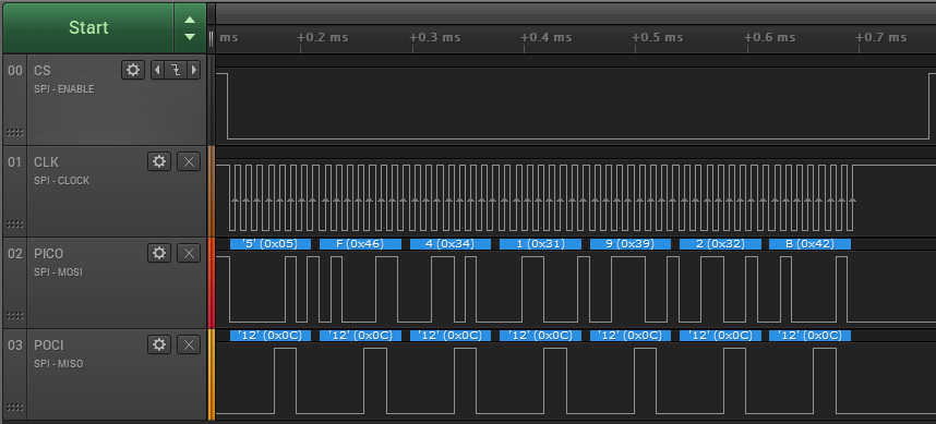
Similar transactions can be captured for the other two data types.
Task 3. Modify SPI Controller Example Project to Configure DAC
In this task, you will build upon things you learned or discovered in the previous sections and modify the SPI controller code to configure a SPI peripheral, the DAC8311 on the BOOSTXL-AUDIO BoosterPack. Don't worry about where to start. We will guide you through those steps.
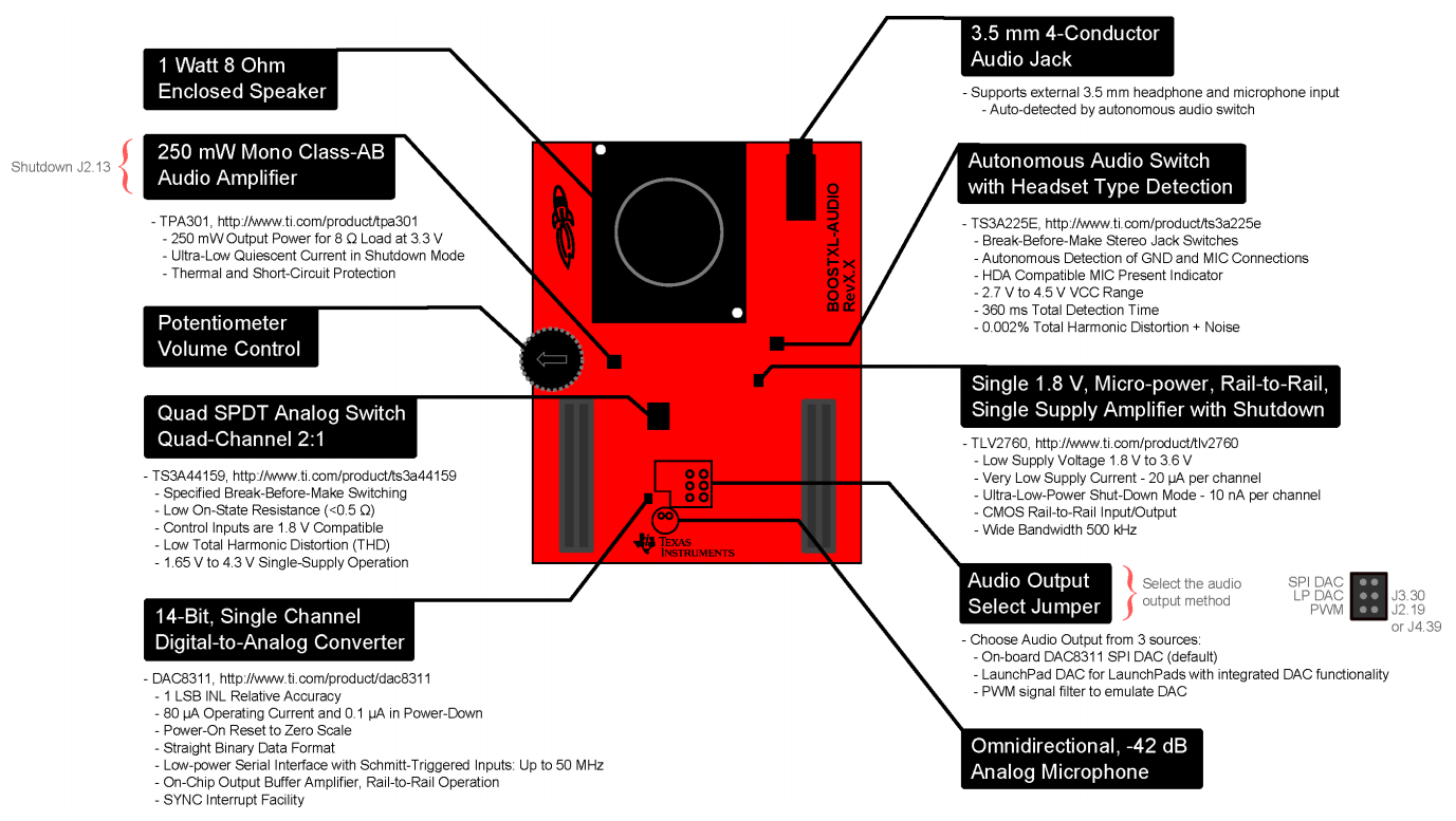
The BOOSTXL-AUDIO BoosterPack supports using the DAC8311 and TPA301 audio power amplifier to output audio through an onboard speaker. However, you will be configuring the DAC8311 to generate a DC voltage for this task. The DAC8311 is a 14-bit low-power single-channel linear-voltage-output DAC.
BoosterPack Overview
NOTE
Before using the BOOSTXL-AUDIO, remove the Audio Output Select Jumper (J5). Then, plug the BoosterPack into the SPI Controller LaunchPad.
To configure the DAC8311 using the SPI controller, here are a some things to keep in mind:
- Do the LaunchPad's SPI pins used in the previous tasks match up to the BoosterPack's SPI pins?
- How many pins are required for the DAC's SPI interface?
- What are the DAC's SPI clock phase and polarity?
- Should the data be sent MSB or LSB first?
- How many control and data registers are there?
- What size are the registers?
- How to control and configure the DAC to operate?
To help answer these questions, refer to the following documents:
- Open the DAC8311 datasheet and find the SPI interface specifications, control and data registers and more.
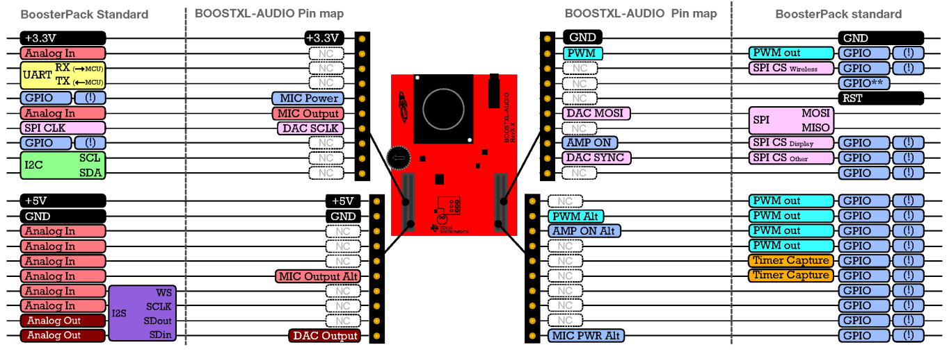
Open the BOOSTXL-AUDIO user's guide and check the header connections and pin functions.
BoosterPack Pinout
Task 3. Software Modifications
The DAC8311's SPI interface is described in the Programming section of the DAC8311 datasheet.
How many wires are required for the DAC's SPI interace?
This task does not require jumper wires for the SPI interface connections because the BoosterPack is plugged directly into the SPI Controller LaunchPad, but it is important to know if those connections are correct and understand which connections are required. Modify the SPI controller's initialization code to support the DAC8311's SPI peripheral interface.
Which eUSCI module must be used with this BoosterPack?
You probably noticed that the DAC8311 does not send data back to the SPI controller, so there is no BoosterPack connection for the SPI POCI pin. The MSP430 SPI controller interface is similar to the 68HC11 microcontroller example in the Application Information section of the DAC8311 datasheet.
MCU to DAC8x11 Interface
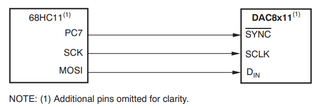
The MSP430's eUSCI module does not support a 2-pin SPI mode, so the default 3-pin SPI mode is not changed.
- MSP430's chip select (GPIO) → DAC's !SYNC
- MSP430's CLK → DAC's SCLK
- MSP430's PICO → DAC's DIN
- MSP430's POCI → Not connected
The inactive state of the DAC8311's SPI clock is low, so remove UCCKPL from the UCA1CTLW0 register settings to ensure the clock polarity between the SPI controller and peripheral matches.
You can keep the 100kHz SPI clock frequency from Task 2, or you can increase the clock frequency by decreasing the value of UCA1BRW.
The DAC8311's SPI clock frequency can be as high as 50MHz, but always remember to refer to the MSP430FR2433's datasheet and find the eUSCI module's maximum input clock frequency in SPI controller mode.
    void initSPI()
    {
        // Clock polarity select: inactive state is low, MSB first
        // 8-bit data, Synchronous, Master mode, 3-pin SPI, BRCLK source: SMCLK
        UCA1CTLW0 = UCSWRST;                    // **Put eUSCI module in reset**
        UCA1CTLW0 |= UCMSB | UCSYNC |
                    UCMST | UCSSEL__SMCLK;
        UCA1BRW = 80;                           // BRCLK / UCBRx = UCxCLK
                                                // 8MHz  / 80    = 100kHz
        UCA1CTLW0 &= ~UCSWRST;                  // **Initialize eUSCI module**
        UCA1IE |= UCRXIE;                       // Enable eUSCI0 RX interrupt
    }
Let's move on to controlling the DAC8311 and configuring the output voltage. The DAC8311 has a single input register that contains control bits (PD1 and PD0) and data bits (D13 to D0). It supports four separate modes of operation, and these modes are programmable by setting the control bits. We want the device to operate in Normal mode.
What are the control bit settings for the DAC's Normal mode?
Next, calculate the data bits (D13 to D0) to output a specific voltage by referring to the equation in the Feature Description section of the DAC8311 datasheet. Combine the two control bits and fourteen data bits into a single 16-bit value that can be sent from the SPI controller to the DAC8311. You will need to populate a MasterTypeX[] array with two bytes in hexadecimal format that represents the combined 16-bit value for the DAC8311's input register.
What MasterTypeX[] array would be the easiest to use for sending two bytes?
Here is a working example for a DAC output voltage of 2.5V. The DAC's input register should be 12412 (decimal) or 0x307C (hexadecimal).
    //uint8_t MasterType1 [TYPE_1_LENGTH] = {8, 9};
    uint8_t MasterType1 [TYPE_1_LENGTH] = {0x30, 0x7C};
At this point, you have updated the eUSCI SPI settings, determined the correct control and data bits and prepared to write the data array. Next, comment out the unused read and write functions.
Here is a working example.
    // CPU wakes up on button press, starts communication
    //SPI_Master_ReadReg(CMD_TYPE_2_SLAVE, TYPE_2_LENGTH);
    //CopyArray(ReceiveBuffer, SlaveType2, TYPE_2_LENGTH);

    //SPI_Master_ReadReg(CMD_TYPE_1_SLAVE, TYPE_1_LENGTH);
    //CopyArray(ReceiveBuffer, SlaveType1, TYPE_1_LENGTH);

    //SPI_Master_ReadReg(CMD_TYPE_0_SLAVE, TYPE_0_LENGTH);
    //CopyArray(ReceiveBuffer, SlaveType0, TYPE_0_LENGTH);

    //SPI_Master_WriteReg(CMD_TYPE_2_MASTER, MasterType2, TYPE_2_LENGTH);
    SPI_Master_WriteReg(CMD_TYPE_1_MASTER, MasterType1, TYPE_1_LENGTH);
    //SPI_Master_WriteReg(CMD_TYPE_0_MASTER, MasterType0, TYPE_0_LENGTH);
The last step is to modify the SPI_Master_WriteReg() function to prevent sending the CMD_TYPE_X_MASTER command before the MasterTypeX[] array.
The DAC8311 has only one input register, so it does not need a register address.
However, you will need to figure out how to trigger the SPI ISR to send the MasterTypeX[] array.
Here is a working example. Commenting out SendUCA1Data(TransmitRegAddr) prevents CMD_TYPE_1_MASTER from getting sent, but it also prevents the code from entering the SPI ISR.
So, we add UCA1IFG |= UCRXIFG to manually trigger the SPI ISR and enter the state machine.
In the SPI ISR, the code enters the TX_REG_ADDRESS_MODE state but skips the if (RXByteCtr) statement because RXByteCtr = 0.
Instead, the code enters the else statement to start sending the bytes in the MasterType1[] array.
    SPI_Mode SPI_Master_WriteReg(uint8_t reg_addr, uint8_t *reg_data, uint8_t count)
    {
        MasterMode = TX_REG_ADDRESS_MODE;
        TransmitRegAddr = reg_addr;

        // Copy register data to TransmitBuffer
        CopyArray(reg_data, TransmitBuffer, count);

        TXByteCtr = count;
        RXByteCtr = 0;
        ReceiveIndex = 0;
        TransmitIndex = 0;

        SLAVE_CS_OUT &= ~(SLAVE_CS_PIN);
        //SendUCA1Data(TransmitRegAddr);
        UCA1IFG |= UCRXIFG;

        __bis_SR_register(CPUOFF + GIE);        // Enter LPM0 w/interrupts enabled

        SLAVE_CS_OUT |= SLAVE_CS_PIN;
        return MasterMode;
    }
To verify the DAC8311's output voltage, build the code and program the SPI Controller LaunchPad. Run the code and press the S1 button on the LaunchPad to write the 16-bit value to the DAC8311.
NOTE
Even if you populate the Audio Output Select Jumper (J5) on the SPI DAC header and enable the audio power amplifier, no audio will be heard from the speaker after completing this task because a DC voltage is generated by the DAC. Capacitor (C11) on the BoosterPack blocks DC signals to the input of the audio power amplifier. The schematic can be found in the BOOSTXL-AUDIO user's guide. To generate an audio signal, you would need to vary the DAC output voltage over time to generate an AC signal. This functionality is demonstrated by the BOOSTXL-AUDIO software examples.
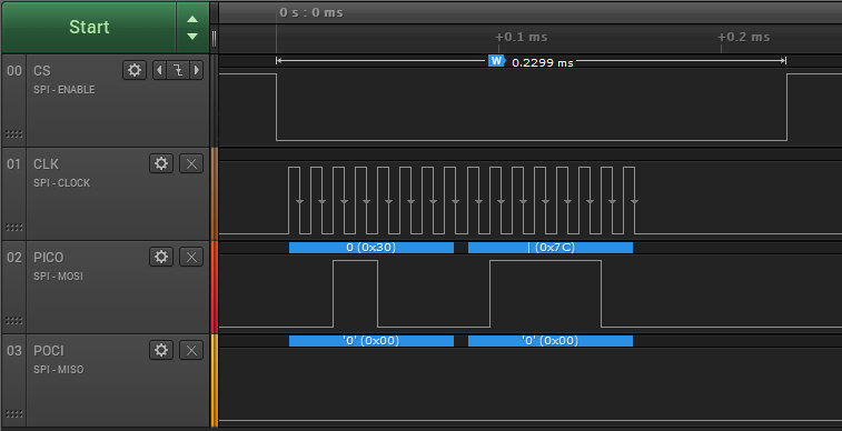
If you have a logic analyzer, you can capture the SPI communication between the SPI controller and the DAC.
Were only two bytes sent? Did those bytes match the MasterType1[] array contents? Here's an example.
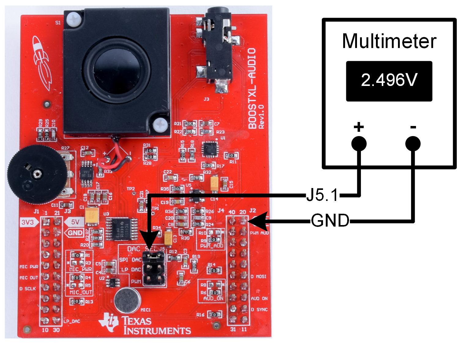
Take your multimeter and measure the DAC8311's output voltage.
It should be very close to the voltage that you specified earlier in this task.
You can always change the two bytes in the MasterType1[] array and repeat this process to adjust the output voltage.
Hopefully you got everything to work! If not, here are a couple of things to try.
Here is the complete solution.
    //******************************************************************************
    //   MSP430FR243x Demo - eUSCI_A1, 4-Wire SPI Master multiple-byte RX/TX
    //
    //   Description: SPI master communicates with SPI slave receiving and sending
    //   3 different messages of different length. SPI master will initially wait
    //   for a port interrupt in LPM0 mode before starting the SPI communication.
    //   SPI master will enter LPM0 mode while waiting for the messages to be
    //   received/sent using SPI interrupt.
    //   ACLK = NA, MCLK = DCO = 16MHz, SMCLK = MCLK / 2 = 8MHz
    //
    //
    //                    MSP430FR2433
    //                 -----------------
    //            /|\ |             P1.1|-> Comms LED2
    //             |  |                 |
    //             ---|RST          P2.2|-> Slave Reset (GPIO)
    //                |                 |
    //                |             P2.6|-> Data Out (UCA1SIMO)
    //                |                 |
    //                |             P2.5|<- Data In (UCA1SOMI)
    //    Button S1 ->|P2.3             |
    //                |             P2.4|-> Serial Clock Out (UCA1CLK)
    //  Button LED1 <-|P1.0             |
    //                |             P2.1|-> Slave Chip Select (GPIO)
    //
    //   James Evans
    //   Texas Instruments Inc.
    //   May 2021
    //   Built with CCS v10.3
    //******************************************************************************

    #include <msp430.h>
    #include <stdint.h>

    //******************************************************************************
    // Pin Config ******************************************************************
    //******************************************************************************

    #define SLAVE_CS_OUT            P2OUT
    #define SLAVE_CS_DIR            P2DIR
    #define SLAVE_CS_PIN            BIT1

    #define SLAVE_RST_OUT           P2OUT
    #define SLAVE_RST_DIR           P2DIR
    #define SLAVE_RST_PIN           BIT2

    #define BUTTON_DIR              P2DIR
    #define BUTTON_OUT              P2OUT
    #define BUTTON_REN              P2REN
    #define BUTTON_PIN              BIT3
    #define BUTTON_IES              P2IES
    #define BUTTON_IE               P2IE
    #define BUTTON_IFG              P2IFG
    #define BUTTON_VECTOR           PORT2_VECTOR

    #define BUTTON_LED_OUT          P1OUT
    #define BUTTON_LED_DIR          P1DIR
    #define BUTTON_LED_PIN          BIT0

    #define COMMS_LED_OUT           P1OUT
    #define COMMS_LED_DIR           P1DIR
    #define COMMS_LED_PIN           BIT1


    //******************************************************************************
    // Example Commands ************************************************************
    //******************************************************************************

    #define DUMMY                   0xFF

    /* CMD_TYPE_X_SLAVE are example commands the master sends to the slave.
    * The slave will send example SlaveTypeX buffers in response.
    *
    * CMD_TYPE_X_MASTER are example commands the master sends to the slave.
    * The slave will initialize itself to receive MasterTypeX example buffers.
    * */

    #define CMD_TYPE_0_SLAVE        0
    #define CMD_TYPE_1_SLAVE        1
    #define CMD_TYPE_2_SLAVE        2

    #define CMD_TYPE_0_MASTER       3
    #define CMD_TYPE_1_MASTER       4
    #define CMD_TYPE_2_MASTER       5

    #define TYPE_0_LENGTH           1
    #define TYPE_1_LENGTH           2
    #define TYPE_2_LENGTH           6

    #define MAX_BUFFER_SIZE         20

    /* MasterTypeX are example buffers initialized in the master, they will be
    * sent by the master to the slave.
    * SlaveTypeX are example buffers initialized in the slave, they will be
    * sent by the slave to the master.
    * */

    uint8_t MasterType0 [TYPE_0_LENGTH] = {0x11};
    //uint8_t MasterType1 [TYPE_1_LENGTH] = {8, 9};
    uint8_t MasterType1 [TYPE_1_LENGTH] = {0x30, 0x7C};
    uint8_t MasterType2 [TYPE_2_LENGTH] = {'F', '4', '1', '9', '2', 'B'};

    uint8_t SlaveType2 [TYPE_2_LENGTH]  = {0};
    uint8_t SlaveType1 [TYPE_1_LENGTH]  = {0};
    uint8_t SlaveType0 [TYPE_0_LENGTH]  = {0};


    //******************************************************************************
    // General SPI State Machine ***************************************************
    //******************************************************************************

    typedef enum SPI_ModeEnum
    {
        IDLE_MODE,
        TX_REG_ADDRESS_MODE,
        RX_REG_ADDRESS_MODE,
        TX_DATA_MODE,
        RX_DATA_MODE,
        TIMEOUT_MODE
    } SPI_Mode;

    /* Used to track the state of the software state machine*/
    SPI_Mode MasterMode = IDLE_MODE;

    /* The Register Address/Command to use*/
    uint8_t TransmitRegAddr = 0;

    /* ReceiveBuffer: Buffer used to receive data in the ISR
    * RXByteCtr: Number of bytes left to receive
    * ReceiveIndex: The index of the next byte to be received in ReceiveBuffer
    * TransmitBuffer: Buffer used to transmit data in the ISR
    * TXByteCtr: Number of bytes left to transfer
    * TransmitIndex: The index of the next byte to be transmitted in TransmitBuffer
    * */
    uint8_t ReceiveBuffer[MAX_BUFFER_SIZE]  = {0};
    uint8_t RXByteCtr = 0;
    uint8_t ReceiveIndex = 0;
    uint8_t TransmitBuffer[MAX_BUFFER_SIZE] = {0};
    uint8_t TXByteCtr = 0;
    uint8_t TransmitIndex = 0;

    /* SPI Write and Read Functions */

    /* For slave device, writes the data specified in *reg_data
    *
    * reg_addr: The register or command to send to the slave.
    *           Example: CMD_TYPE_0_MASTER
    * *reg_data: The buffer to write
    *           Example: MasterType0
    * count: The length of *reg_data
    *           Example: TYPE_0_LENGTH
    *  */
    SPI_Mode SPI_Master_WriteReg(uint8_t reg_addr, uint8_t *reg_data, uint8_t count);

    /* For slave device, read the data specified in slaves reg_addr.
    * The received data is available in ReceiveBuffer
    *
    * reg_addr: The register or command to send to the slave.
    *           Example: CMD_TYPE_0_SLAVE
    * count: The length of data to read
    *           Example: TYPE_0_LENGTH
    *  */
    SPI_Mode SPI_Master_ReadReg(uint8_t reg_addr, uint8_t count);
    void CopyArray(uint8_t *source, uint8_t *dest, uint8_t count);
    void SendUCA1Data(uint8_t val);

    void SendUCA1Data(uint8_t val)
    {
        while (!(UCA1IFG & UCTXIFG));           // USCI_A1 TX buffer ready?
        UCA1TXBUF = val;
    }

    void CopyArray(uint8_t *source, uint8_t *dest, uint8_t count)
    {
        uint8_t copyIndex = 0;
        for (copyIndex = 0; copyIndex < count; copyIndex++)
        {
            dest[copyIndex] = source[copyIndex];
        }
    }

    SPI_Mode SPI_Master_WriteReg(uint8_t reg_addr, uint8_t *reg_data, uint8_t count)
    {
        MasterMode = TX_REG_ADDRESS_MODE;
        TransmitRegAddr = reg_addr;

        // Copy register data to TransmitBuffer
        CopyArray(reg_data, TransmitBuffer, count);

        TXByteCtr = count;
        RXByteCtr = 0;
        ReceiveIndex = 0;
        TransmitIndex = 0;

        SLAVE_CS_OUT &= ~(SLAVE_CS_PIN);
        //SendUCA1Data(TransmitRegAddr);
        UCA1IFG |= UCRXIFG;

        __bis_SR_register(CPUOFF + GIE);        // Enter LPM0 w/interrupts enabled

        SLAVE_CS_OUT |= SLAVE_CS_PIN;
        return MasterMode;
    }

    SPI_Mode SPI_Master_ReadReg(uint8_t reg_addr, uint8_t count)
    {
        MasterMode = TX_REG_ADDRESS_MODE;
        TransmitRegAddr = reg_addr;
        RXByteCtr = count;
        TXByteCtr = 0;
        ReceiveIndex = 0;
        TransmitIndex = 0;

        SLAVE_CS_OUT &= ~(SLAVE_CS_PIN);
        SendUCA1Data(TransmitRegAddr);

        __bis_SR_register(CPUOFF + GIE);        // Enter LPM0 w/interrupts enabled

        SLAVE_CS_OUT |= SLAVE_CS_PIN;
        return MasterMode;
    }


    //******************************************************************************
    // Device Initialization *******************************************************
    //******************************************************************************

    void initSPI()
    {
        // Clock polarity select: inactive state is low, MSB first
        // 8-bit data, Synchronous, Master mode, 3-pin SPI, BRCLK source: SMCLK
        UCA1CTLW0 = UCSWRST;                    // **Put eUSCI module in reset**
        UCA1CTLW0 |= UCMSB | UCSYNC |
                    UCMST | UCSSEL__SMCLK;
        UCA1BRW = 80;                           // BRCLK / UCBRx = UCxCLK
                                                // 8MHz  / 80    = 100kHz
        UCA1CTLW0 &= ~UCSWRST;                  // **Initialize eUSCI module**
        UCA1IE |= UCRXIE;                       // Enable eUSCI0 RX interrupt
    }

    void initGPIO()
    {
        // Configure LEDs and buttons
        COMMS_LED_DIR |= COMMS_LED_PIN;
        COMMS_LED_OUT &= ~COMMS_LED_PIN;

        BUTTON_LED_DIR |= BUTTON_LED_PIN;
        BUTTON_LED_OUT &= ~BUTTON_LED_PIN;

        // Configure eUSCI pins
        P2SEL0 |= BIT4 | BIT5 | BIT6;
        P2SEL1 &= ~(BIT4 | BIT5 | BIT6);

        SLAVE_RST_DIR |= SLAVE_RST_PIN;
        SLAVE_RST_OUT |= SLAVE_RST_PIN;

        SLAVE_CS_DIR |= SLAVE_CS_PIN;
        SLAVE_CS_OUT |= SLAVE_CS_PIN;

        // Button to initiate transfer
        BUTTON_DIR &= ~BUTTON_PIN;              // Button input
        BUTTON_OUT |= BUTTON_PIN;               // Button pull up
        BUTTON_REN |= BUTTON_PIN;               // Button pull up/down resistor enable
        BUTTON_IES |= BUTTON_PIN;               // Button high-to-low edge

        // Disable the GPIO power-on default high-impedance mode to activate
        // previously configured port settings
        PM5CTL0 &= ~LOCKLPM5;

        // Must be done after clearing LOCKLPM5
        BUTTON_IFG &= ~BUTTON_PIN;              // Button IFG cleared
        BUTTON_IE  |= BUTTON_PIN;               // Button interrupt enabled
    }

    void initClockTo16MHz()
    {
        // Configure one FRAM waitstate as required by the device datasheet for MCLK
        // operation beyond 8MHz _before_ configuring the clock system.
        FRCTL0 = FRCTLPW | NWAITS_1;

        __bis_SR_register(SCG0);    // Disable FLL
        CSCTL3 |= SELREF__REFOCLK;  // Set REFO as FLL reference source
        CSCTL0 = 0;                 // Clear DCO and MOD registers
        CSCTL1 &= ~(DCORSEL_7);     // Clear DCO frequency select bits first
        CSCTL1 |= DCORSEL_5;        // Set DCO = 16MHz
        CSCTL2 = FLLD_0 + 487;      // set to fDCOCLKDIV = (FLLN + 1)*(fFLLREFCLK/n)
                                    //                   = (487  + 1)*(32.768 kHz/1)
                                    //                   = 16MHz

        __delay_cycles(3);
        __bic_SR_register(SCG0);                    // Enable FLL
        while(CSCTL7 & (FLLUNLOCK0 | FLLUNLOCK1));  // FLL locked

        CSCTL5 |= DIVM_0 | DIVS_1;                  // MCLK = DCOCLK = 16MHz,
                                                    // SMCLK = MCLK/2 = 8MHz
    }


    //******************************************************************************
    // Main ************************************************************************
    // Send and receive three messages containing the example commands *************
    //******************************************************************************

    int main(void)
    {
        // Stop watchdog timer
        WDTCTL = WDTPW | WDTHOLD;

        // Initialize device
        initClockTo16MHz();
        initGPIO();
        initSPI();

        while(1)
        {
            // Reset slave after initializing eUSCI pins
            COMMS_LED_OUT &= ~COMMS_LED_PIN;        // Turn off comms LED
            SLAVE_RST_OUT &= ~SLAVE_RST_PIN;        // Reset slave
            __delay_cycles(100000);                 // Wait
            SLAVE_RST_OUT |= SLAVE_RST_PIN;         // Release slave
            __delay_cycles(100000);                 // Wait for slave to initialize
            COMMS_LED_OUT |= COMMS_LED_PIN;         // Turn on comms LED

            // Enter LPM0 w/interrupts enabled
            __bis_SR_register(LPM0_bits + GIE);

            // CPU wakes up on button press, starts communication
    //        SPI_Master_ReadReg(CMD_TYPE_2_SLAVE, TYPE_2_LENGTH);
    //        CopyArray(ReceiveBuffer, SlaveType2, TYPE_2_LENGTH);
    //
    //        SPI_Master_ReadReg(CMD_TYPE_1_SLAVE, TYPE_1_LENGTH);
    //        CopyArray(ReceiveBuffer, SlaveType1, TYPE_1_LENGTH);
    //
    //        SPI_Master_ReadReg(CMD_TYPE_0_SLAVE, TYPE_0_LENGTH);
    //        CopyArray(ReceiveBuffer, SlaveType0, TYPE_0_LENGTH);

            //SPI_Master_WriteReg(CMD_TYPE_2_MASTER, MasterType2, TYPE_2_LENGTH);
            SPI_Master_WriteReg(CMD_TYPE_1_MASTER, MasterType1, TYPE_1_LENGTH);
            //SPI_Master_WriteReg(CMD_TYPE_0_MASTER, MasterType0, TYPE_0_LENGTH);

            // Re-enable button to repeat transfer
            BUTTON_IE  |= BUTTON_PIN;               // Button interrupt enabled
            BUTTON_LED_OUT &= ~BUTTON_LED_PIN;      // Turn off button LED
        }
    }


    //******************************************************************************
    // SPI Interrupt ***************************************************************
    //******************************************************************************

    #if defined(__TI_COMPILER_VERSION__) || defined(__IAR_SYSTEMS_ICC__)
    #pragma vector=USCI_A1_VECTOR
    __interrupt void USCI_A1_ISR(void)
    #elif defined(__GNUC__)
    void __attribute__ ((interrupt(USCI_A1_VECTOR))) USCI_A1_ISR (void)
    #else
    #error Compiler not supported!
    #endif
    {
        uint8_t uca1_rx_val = 0;
        switch(__even_in_range(UCA1IV, USCI_SPI_UCTXIFG))
        {
            case USCI_NONE: break;
            case USCI_SPI_UCRXIFG:
                uca1_rx_val = UCA1RXBUF;
                UCA1IFG &= ~UCRXIFG;
                switch (MasterMode)
                {
                    case TX_REG_ADDRESS_MODE:
                        if (RXByteCtr)
                        {
                            // Need to start receiving now
                            MasterMode = RX_DATA_MODE;

                            // Send dummy byte to start
                            __delay_cycles(5000);
                            SendUCA1Data(DUMMY);
                        }
                        else
                        {
                            // Continue to transmission
                            MasterMode = TX_DATA_MODE;

                            // Send first byte
                            SendUCA1Data(TransmitBuffer[TransmitIndex++]);
                            TXByteCtr--;
                        }
                        break;

                    case TX_DATA_MODE:
                        if (TXByteCtr)
                        {
                            // Send additional byte
                            SendUCA1Data(TransmitBuffer[TransmitIndex++]);
                            TXByteCtr--;
                        }
                        else
                        {
                            // Done with transmission
                            MasterMode = IDLE_MODE;
                            __bic_SR_register_on_exit(CPUOFF);  // Exit LPM0
                        }
                        break;

                    case RX_DATA_MODE:
                        if (RXByteCtr)
                        {
                            // Store received byte
                            ReceiveBuffer[ReceiveIndex++] = uca1_rx_val;
                            RXByteCtr--;
                        }
                        if (RXByteCtr == 0)
                        {
                            // Done with reception
                            MasterMode = IDLE_MODE;
                            __bic_SR_register_on_exit(CPUOFF);  // Exit LPM0
                        }
                        else
                        {
                            // Send dummy byte to receive next byte
                            SendUCA1Data(DUMMY);
                        }
                        break;

                    default:
                        __no_operation();
                        break;
                }
                __delay_cycles(1000);
                break;
            case USCI_SPI_UCTXIFG:
                break;
            default: break;
        }
    }


    //******************************************************************************
    // PORT Interrupt **************************************************************
    // Interrupt occurs on button press and initiates the SPI data transfer ********
    //******************************************************************************

    #if defined(__TI_COMPILER_VERSION__) || defined(__IAR_SYSTEMS_ICC__)
    #pragma vector=BUTTON_VECTOR
    __interrupt void Button_ISR(void)
    #elif defined(__GNUC__)
    void __attribute__ ((interrupt(BUTTON_VECTOR))) Button_ISR (void)
    #else
    #error Compiler not supported!
    #endif
    {
        // Check if button was pressed
        if (BUTTON_IFG & BUTTON_PIN)
        {
            // Disable button
            BUTTON_LED_OUT |= BUTTON_LED_PIN;       // Button LED on
            BUTTON_IFG &= ~BUTTON_PIN;              // Button IFG cleared
            BUTTON_IE &= ~BUTTON_PIN;               // Button IFG disabled
            __delay_cycles(1000);

            // Wake up CPU to start communication
            __bic_SR_register_on_exit(LPM0_bits);   // Exit LPM0
        }
    }
Here are some tips:
- Did you forget to push the S1 button on the LaunchPad to initiate the SPI communication?
- Did you remove the Audio Output Select Jumper (J5)?
- Did you organize the data in the array with the MSB first?
- Did you make sure the PD1 and PD0 control bits are always set to 0?
- Do the SPI protocol analyzer settings in your logic analyzer GUI match the SPI clock phase and polarity?
- If you are using a multimeter to measure the DAC8311's output voltage, are you probing the correct pins on the BoosterPack?
- Are your multimeter probes making adequate contact with the BoosterPack pins?
Task 4. Modify SPI Peripheral Example Project to Emulate DAC
In Task 3, you modified the SPI controller code to work with the DAC8311, so by now, you should feel more comfortable creating SPI controller code that communicates with most SPI peripheral devices. In this task, you will modify the SPI peripheral code to emulate the DAC8311 in a very simple way. The MSP430FR2433 does not feature an integrated DAC like the MSP430FR2355, so we will improvise and create a simple 1-bit DAC using a GPIO to turn an LED on or off.
Task 4. Software Modifications
The requirements for the SPI peripheral are:
- Read the data bits (D13 to D0) written by the SPI controller and store them in an array
- Analyze the data bits
- Control the LED output accordingly
If the data bits are greater than 0, turn on the LED. Otherwise, turn off the LED. This functionality emulates the output of a 1-bit DAC.
NOTE
We are assuming both control bits (PD1 and PD0) are set to 0, which ensures the DAC operates in Normal mode.
The SPI peripheral code from Task 1 expects a command for the first byte received, but remember we modified the SPI controller code to skip sending the command. Modify the SPI peripheral code so it receives the first data byte rather than a command. There are several ways to accomplish this task.
Here is a working example.
First, change the SPI ISR code in the RX_REG_ADDRESS_MODE case to store the first data byte.
Notice how the argument for the function SPI_Slave_ProcessCMD() was changed to CMD_TYPE_1_MASTER to initialize RXByteCtr and select the next mode.
The same approach was used for the function SPI_Slave_TransactionDone() in the RX_DATA_MODE case.
    #if defined(__TI_COMPILER_VERSION__) || defined(__IAR_SYSTEMS_ICC__)
    #pragma vector=USCI_A1_VECTOR
    __interrupt void USCI_A1_ISR(void)
    #elif defined(__GNUC__)
    void __attribute__ ((interrupt(USCI_A1_VECTOR))) USCI_A1_ISR (void)
    #else
    #error Compiler not supported!
    #endif
    {
        uint8_t uca1_rx_val = 0;
        switch(__even_in_range(UCA1IV, USCI_SPI_UCTXIFG))
        {
            case USCI_NONE: break;
            case USCI_SPI_UCRXIFG:
                uca1_rx_val = UCA1RXBUF;
                UCA1IFG &= ~UCRXIFG;
                switch (SlaveMode)
                {
                    case (RX_REG_ADDRESS_MODE):
                        //ReceiveRegAddr = uca1_rx_val;
                        SPI_Slave_ProcessCMD(CMD_TYPE_1_MASTER);
                        ReceiveBuffer[ReceiveIndex++] = uca1_rx_val;
                        RXByteCtr--;
                        break;
                    case (RX_DATA_MODE):
                        // Store received byte
                        ReceiveBuffer[ReceiveIndex++] = uca1_rx_val;
                        RXByteCtr--;
                        if (RXByteCtr == 0)
                        {
                            // Done with reception
                            SlaveMode = RX_REG_ADDRESS_MODE;
                            SPI_Slave_TransactionDone(CMD_TYPE_1_MASTER);
                        }
                        break;
                    case (TX_DATA_MODE):
                        if (TXByteCtr > 0)
                        {
                            // Send additional byte
                            SendUCA1Data(TransmitBuffer[TransmitIndex++]);
                            TXByteCtr--;
                        }
                        if (TXByteCtr == 0)
                        {
                            // Done with transmission
                            SlaveMode = RX_REG_ADDRESS_MODE;
                            SPI_Slave_TransactionDone(ReceiveRegAddr);
                        }
                        break;
                    default:
                        __no_operation();
                        break;
                    }
                break;
            case USCI_SPI_UCTXIFG:
                break;
            default: break;
        }
    }
The SPI_Slave_TransactionDone() function is called when both bytes have been received from the SPI controller.
Add code to this function to evaluate the data bits after receiving them from the SPI controller and control the LED output accordingly.
Here is a working example.
    void SPI_Slave_TransactionDone(uint8_t cmd)
    {
        switch (cmd)
        {
            // Slave device ID was sent (this device's ID)
            case (CMD_TYPE_0_SLAVE):
                break;

            // Slave device time was sent (this device's time)
            case (CMD_TYPE_1_SLAVE):
                break;

            // Slave device location was sent (this device's location)
            case (CMD_TYPE_2_SLAVE):
                break;

            case (CMD_TYPE_0_MASTER):
                CopyArray(ReceiveBuffer, MasterType0, TYPE_0_LENGTH);
                break;

            case (CMD_TYPE_1_MASTER):
                CopyArray(ReceiveBuffer, MasterType1, TYPE_1_LENGTH);

                // Evaluate the data bits (ignore the control bits)
                if ((MasterType1[0] > 0) || (MasterType1[1] > 0))
                {
                    // Turn on LED1
                    LED_OUT |= LED0_PIN;
                }
                else
                {
                    // Turn off LED1
                    LED_OUT &= ~LED0_PIN;
                }
                break;

            case (CMD_TYPE_2_MASTER):
                CopyArray(ReceiveBuffer, MasterType2, TYPE_2_LENGTH);
                break;

            default:
                __no_operation();
                break;
        }
    }
Did you forget about the SPI clock polarity? Remember that the DAC uses a different clock polarity than the SPI peripheral code in Task 1.
That's already been updated in the SPI controller code, so change the SPI initialization code by removing UCCKPL from the UCA1CTLW0 register settings.
    void initSPI()
    {
        // Clock polarity select: inactive state is low, MSB first
        // 8-bit data, Synchronous, Slave mode, 4-pin SPI
        UCA1CTLW0 = UCSWRST;                    // **Put eUSCI module in reset**
        UCA1CTLW0 |= UCMSB | UCSYNC |
                    UCMODE_2;
        UCA1CTLW0 &= ~UCSWRST;                  // **Initialize eUSCI module**
        UCA1IE |= UCRXIE;                       // Enable eUSCI0 RX interrupt
    }
Build the SPI peripheral code and program the SPI Peripheral LaunchPad. Run the code and press the S1 button on the SPI Controller LaunchPad to write the 16-bit value to the SPI Peripheral LaunchPad. If the received data bits are greater than 0, LED1 on the SPI Peripheral LaunchPad should turn on.
Now, change the MasterType1[] array in the SPI controller code to send 0x0000 and reprogram the SPI Controller LaunchPad.
Repeat the process and LED1 on the SPI Peripheral LaunchPad should not turn on after pressing the S1 button on the SPI Controller LaunchPad.
Too easy? Try this. Configure the SPI peripheral code to also check the control bits (PD1 and PD0). If they aren't equal to 0, turn off LED1, ignoring the data bits.
Summary
At the end of this lab, you should know:
- Fundametal SPI read and write transactions
- How to use MSP430 as a SPI controller to control a SPI peripheral such as a DAC
- How to use MSP430 as a SPI peripheral to emulate a DAC
This work is licensed under a Creative Commons Attribution-NonCommercial-NoDerivatives 4.0 International License.