Introduction
This lab demonstrates generating PWM(pulse-width-modulated) signals using the MSP-EXP430FR2433 and its integrated Timer_A module in different modes. We will demonstrate several timer operating modes to generate different PWM output signals on the MSP430. This lab uses MSP430Ware register level code examples from MSP430Ware.
The lab has 2 tasks consisting of the following activities:
- PWM Signal Output, Up Mode
- PWM Signal Output, Up/Down Mode
Prerequisites
Before we start with this academy, we recommend you to start with the MSP Academy - Timers: Compare Mode first for a better understanding of how the timer works.
Hardware
The following hardware is required for this lab
- MSP-EXP430FR2433 LaunchPad
- A logic analyzer or an oscilloscope is highly recommended to observing the output PWM signal
Software
Installing the software
NOTE:
This software examples used for this lab should be imported from within the TI Resource Explorer. This can be accessed from the web or within a locally in CCS by clicking View->Resource Explorer. Prior to importing a Project, you first need to download MSP430Ware in order to be able to import the examples to the CCS IDE. This may be done when CCS was installed or can be done later by clicking the "Download and Install" icon in the top right. Note that installing MSP430Ware for any project will install ALL labs and content, so this only needs to be done once.
Recommended Resources
These training materials provide a baseline introduction to the hardware. This documentation can be referenced for the MSP430 MCU and the launchpad details.
Overview
This lab introduces generating PWM signals on MSP MCUs by configuring the timer module.
In this lab you will be using one launchpad to output two PWM signals on P1.1 and P1.2, and modify the output mode bits to observe the impact on the output signal.
Getting Started
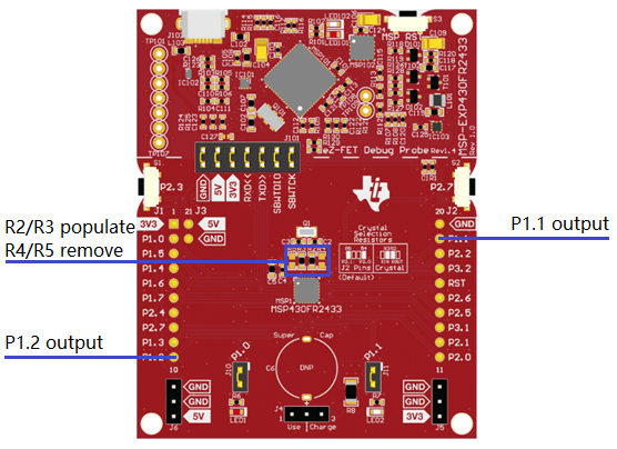
Hardware Setup:
Warning:
This example requires resistors R2/R3 to be populated and R4/R5 to be removed to use the LF XTAL for the MSP430FR2433. Please check your launchpad documentation for the exact specifications to enable the LF XTAL.
Task 1 – PWM Signal Output, Up Mode
This task will show how to generate a PWM waveform with a fixed frequency and duty cycle with a MSP430 timer module. This task is to use TimerA0 to generate a PWM signal in Up mode.
Up Mode Project Overview
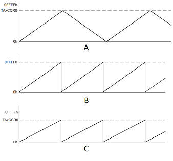
The timer module has four modes of operation: Stop, Up, Continuous, and Up/Down (see below Table). The operating mode is selected with the MC bits.
| MC | Mode | Description |
|---|---|---|
| 00 | Stop | The timer is halted. |
| 01 | Up | The timer repeatedly counts from zero to the value of TAxCCR0. |
| 10 | Continuous | The timer repeatedly counts from zero to 0FFFFh. |
| 11 | Up/down | The timer repeatedly counts from zero up to the value of TAxCCR0 and back down to zero. |
Which of the following image is the Up mode?
Before we make any modifications, let's build and program the msp430 launchpad with the ta0_17.c example to understand what it does.
- Import the ta0_17.c example msp430fr243x_ta0_17.c into CCS from TI Resource Explorer.
MSP430ware→Development Tools→MSP-EXP430FR2433→Peripheral Examples→Register Level→MSP430FR2433→
msp430fr243x_ta0_17.c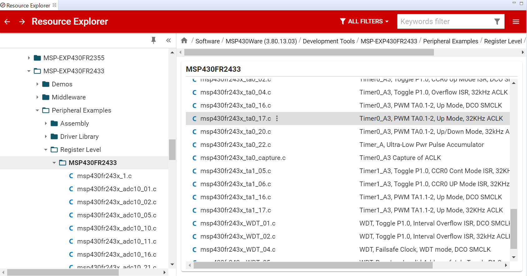
- Click import in the upper right hand corner
- Program the launchpad
Up Mode Code Review
Let's break down this example into three parts: Configuring the GPIO, configuring the clock system, and configuring the timer. After configuring these three modules, the MSP430 will enter LPM3 mode and output the PWM signals.
    //******************************************************************************
    // Main ************************************************************************
    // Configure the clock system setups first. Then configure the timer in UP mode*
    // to output the PWM signal accordingly                                        *
    //******************************************************************************

    void main {
        WDTCTL = WDTPW | WDTHOLD;                         // Stop WDT

        // Configure GPIO
        P1DIR |= BIT1 | BIT2;                             // P1.1 and P1.2 output
        P1SEL1 |= BIT1 | BIT2;                            // P1.1 and P1.2 options select
        P2SEL0 |= BIT0 | BIT1;                            // P2.0~P2.1: crystal pins
        do
        {
            CSCTL7 &= ~(XT1OFFG | DCOFFG);                // Clear XT1 and DCO fault flag
            SFRIFG1 &= ~OFIFG;
        }while (SFRIFG1 & OFIFG);                         // Test oscillator fault flag
        // Disable the GPIO power-on default high-impedance mode to activate
        // previously configured port settings
        PM5CTL0 &= ~LOCKLPM5;

        // Configure clock
        __bis_SR_register(SCG0);                          // disable FLL
        CSCTL3 |= SELREF__REFOCLK;                        // Set REFOCLK as FLL reference source
        CSCTL0 = 0;                                       // clear DCO and MOD registers
        CSCTL1 &= ~(DCORSEL_7);                           // Clear DCO frequency select bits first
        CSCTL1 |= DCORSEL_3;                              // Set DCOCLK = 8MHz
        CSCTL2 = FLLD_1 + 121;                            // FLLD = 1, DCODIV = 4MHz
        __delay_cycles(3);
        __bic_SR_register(SCG0);                          // enable FLL
        while(CSCTL7 & (FLLUNLOCK0 | FLLUNLOCK1));        // Poll until FLL is locked
        CSCTL4 = SELMS__DCOCLKDIV | SELA__XT1CLK;         // set ACLK = XT1 = 32768Hz, DCOCLK as MCLK and SMCLK source
        CSCTL5 |= DIVM0 | DIVS0;                          // SMCLK = MCLK = DCODIV = 1MHz, by default

        // Setup Timer0_A
        TA0CCR0 = 100-1;                                  // PWM Period
        TA0CCTL1 = OUTMOD_7;                              // CCR1 reset/set
        TA0CCR1 = 75;                                     // CCR1 PWM duty cycle
        TA0CCTL2 = OUTMOD_7;                              // CCR2 reset/set
        TA0CCR2 = 25;                                     // CCR2 PWM duty cycle
        TA0CTL = TASSEL_1 | MC_1 | TACLR;                 // ACLK, up mode, clear TAR

        __bis_SR_register(LPM3_bits);                     // Enter LPM3
        __no_operation();                                 // For debug
    }
main()
First we need to configure the GPIO settings. Set the P1.1 and P1.2 as the PWM output pins.
    P1DIR |= BIT1 | BIT2;                             // P1.1 and P1.2 output
    P1SEL1 |= BIT1 | BIT2;                            // P1.1 and P1.2 options select
PWM signal output pin setting
Then set the P2.0 and P2.1 as the external 32.768kHz crystal pins. Then clear the XT1 and DCO fault flags to test if the crystal oscillation correctly. If the crystal does not work correctly, the code will stay in the while loop.
    P2SEL0 |= BIT0 | BIT1;                            // P2.0~P2.1: crystal pins
    do
    {
        CSCTL7 &= ~(XT1OFFG | DCOFFG);                // Clear XT1 and DCO fault flag
        SFRIFG1 &= ~OFIFG;
    }while (SFRIFG1 & OFIFG);                         // Test oscillator fault flag
external crystal setting
Set DCO as 8MHz. Set the external 32.768kHz XT1 as the ACLK source. Set the DCOCLK as the MCLK and SMCLK source.
    __bis_SR_register(SCG0);                          // disable FLL
    CSCTL3 |= SELREF__REFOCLK;                        // Set REFOCLK as FLL reference source
    CSCTL0 = 0;                                       // clear DCO and MOD registers
    CSCTL1 &= ~(DCORSEL_7);                           // Clear DCO frequency select bits first
    CSCTL1 |= DCORSEL_3;                              // Set DCOCLK = 8MHz
    CSCTL2 = FLLD_1 + 121;                            // FLLD = 1, DCODIV = 4MHz
    __delay_cycles(3);
    __bic_SR_register(SCG0);                          // enable FLL
    while(CSCTL7 & (FLLUNLOCK0 | FLLUNLOCK1));        // Poll until FLL is locked
    CSCTL4 = SELMS__DCOCLKDIV | SELA__XT1CLK;         // set ACLK = XT1 = 32768Hz, DCOCLK as MCLK and SMCLK source
    CSCTL5 |= DIVM0 | DIVS0;                          // SMCLK = MCLK = DCODIV = 1MHz, by default
configure clock system
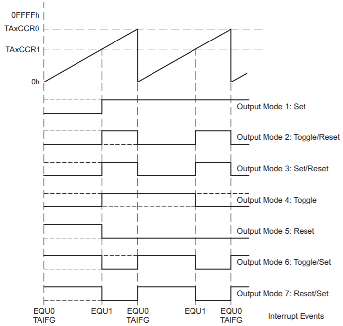
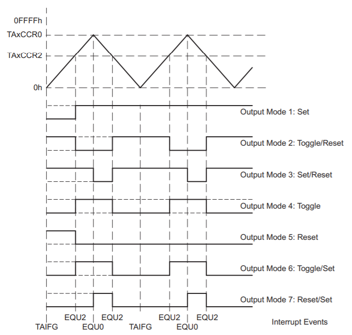
Then set the timerA0 to output a PWM signal. There are 8 output modes that generate signals based on the EQU0 and EQUn signals.
| OUTMOD | Mode | Description |
|---|---|---|
| 000 | Output | The output signal OUTn is defined by the OUT bit. The OUTn signal updates immediately when OUT is updated. |
| 001 | Set | The output is set when the timer counts to the TAxCCRn value. It remains set until a reset of the timer, or until another output mode is selected and affects the output. |
| 010 | Toggle/Reset | The output is toggled when the timer counts to the TAxCCRn value. It is reset when the timer counts to the TAxCCR0 value. |
| 011 | Set/Reset | The output is set when the timer counts to the TAxCCRn value. It is reset when the timer counts to the TAxCCR0 value. |
| 100 | Toggle | The output is toggled when the timer counts to the TAxCCRn value. The output period is double the timer period. |
| 101 | Reset | The output is reset when the timer counts to the TAxCCRn value. It remains reset until another output mode is selected and affects the output. |
| 110 | Toggle/Set | The output is toggled when the timer counts to the TAxCCRn value. It is set when the timer counts to the TAxCCR0 value. |
| 111 | Reset/Set | The output is reset when the timer counts to the TAxCCRn value. It is set when the timer counts to the TAxCCR0 value. |
The OUTn signal is changed when the timer counts up to the TAxCCRn value and rolls from TAxCCR0 to zero, depending on the output mode. Below figure shows an example using TAxCCR0 and TAxCCR1 in Up mode.
In this example, we are using Up mode with Reset/Set output mode to generate the PWM signals. Set ACLK as the timeA0 clock source. Set timerA0 as up mode, clear timerA counter. Set the TA0CCR1 and TA0CCR2 output mode as Reset/Set mode(output mode 7) and configure the PWM duty.
    TA0CCR0 = 100-1;                                  // PWM Period
    TA0CCTL1 = OUTMOD_7;                              // CCR1 reset/set
    TA0CCR1 = 75;                                     // CCR1 PWM duty cycle
    TA0CCTL2 = OUTMOD_7;                              // CCR2 reset/set
    TA0CCR2 = 25;                                     // CCR2 PWM duty cycle
    TA0CTL = TASSEL_1 | MC_1 | TACLR;                 // ACLK, up mode, clear TAR
configure PWM output
Up Mode Logic Captures
Build and download the program to the launchpad. Use a Logic Probe to capture the P1.1 and P1.2 signals. Please think about the folowing two questions before measuring the results.
What's the right answer here?
How to calculate the PWM frequency?
What is the duty of the P1.1 signal?
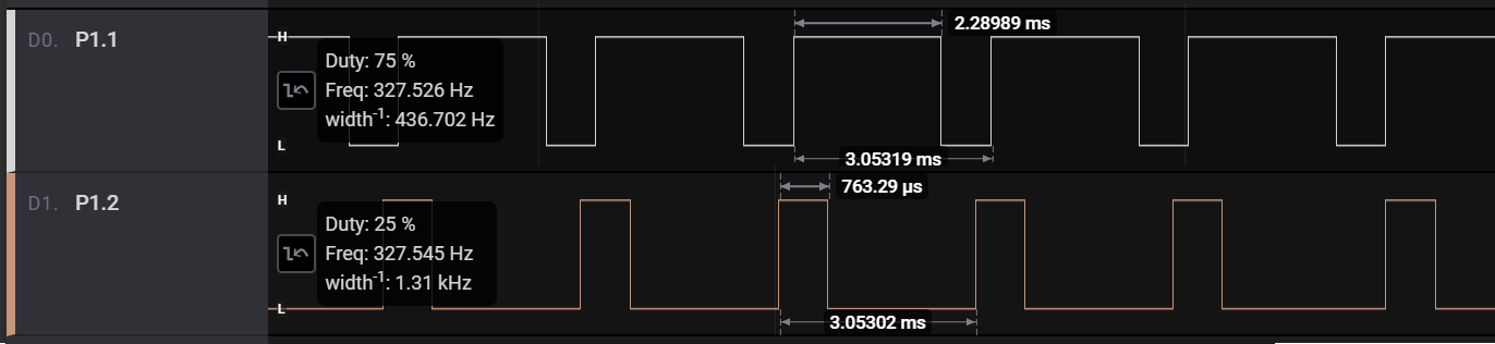
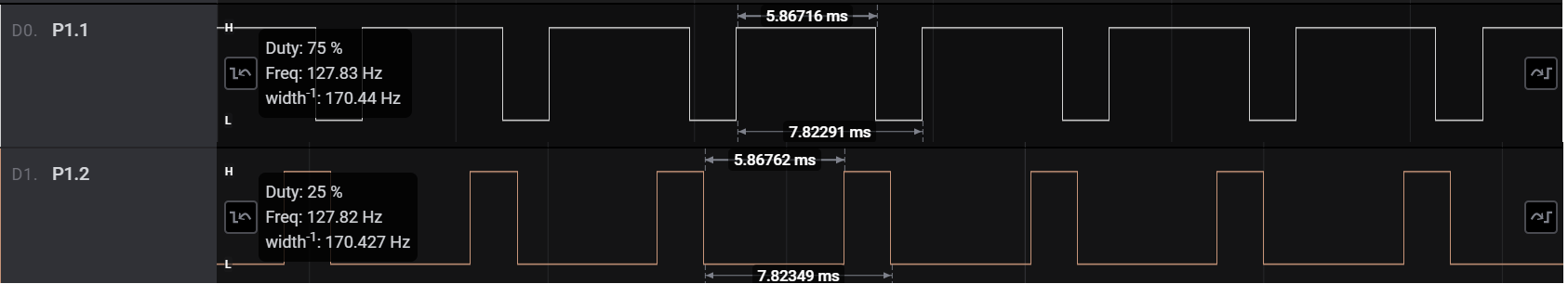
The capture shown here is the P1.1 and P1.2 output PWM signals.
Let's think further about how to generate a PWM signal with a fixed frequency.
How to change the PWM signal frequency?
Yes, that is correct! You can change the PWM signal frequency by changing the TimerA0 clock source's frequency or changing the TA0CCR0 value.
Let's change the TA0CCR0 to (200-1) and see what happens to the output signals.
    TA0CCR0 = 200-1;                                  // Change the PWM frequency here
    TA0CCTL1 = OUTMOD_7;                              // CCR1 reset/set
    TA0CCR1 = 75;                                     // CCR1 PWM duty cycle
    TA0CCTL2 = OUTMOD_7;                              // CCR2 reset/set
    TA0CCR2 = 25;                                     // CCR2 PWM duty cycle
    TA0CTL = TASSEL_1 | MC_1 | TACLR;                 // ACLK, up mode, clear TAR
configure PWM output
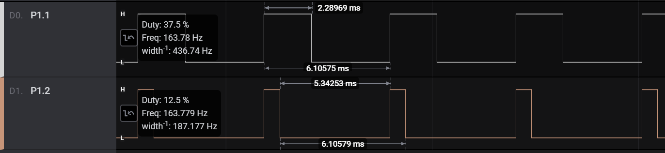
When we change the TA0CCR0 to (200-1), the output signal frequency should be
ACLK frequency ÷ (TA0CCR0 + 1) = 32768 ÷ 200 = 163.84Hz.
And since we have not change the TA0CCR1 and TA0CCR2 value, the PWM duty cycle for P1.1 signal should be
TA0CCR1 ÷ (TA0CCR0 + 1) = 75 ÷ 200 = 0.375.
The PWM duty cycle for P1.2 signal should be
TA0CCR2 ÷ (TA0CCR0 + 1) = 25 ÷ 200 = 0.125.
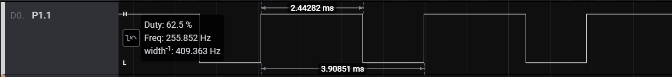
You are now capable to change the PWM signal frequency. Here comes another question, how to get a 256Hz PWM signal with 62.5% duty cycle?
TA0CCR0 + 1 = ACLK frequency ÷ target frequency = 32768 ÷ 256 = 128,
TA0CCR1 = TA0CCR0 × Duty cycle = 128 × 62.5% = 80,
Let's change the code based on the calculation result to get the target signal.
    TA0CCR0 = 128-1;                                  // Set the PWM frequency here
    TA0CCTL1 = OUTMOD_7;                              // CCR1 reset/set
    TA0CCR1 = 80;                                     // Set the PWM duty cycle here
    TA0CTL = TASSEL_1 | MC_1 | TACLR;                 // ACLK, up mode, clear TAR
configure PWM output
The capture shows the P1.1 output signal.
Task 2 – PWM Signal Output, Up/Down Mode
This task is to use TimerA0 to generate a PWM signal in Up/Down mode.
Up/Down Mode Overview
In this task there is no code to modify, so build and program the msp430 launchpad with the ta0_20.c example.
- Import the ta0_20.c example msp430fr243x_ta0_20.c into CCS from TI Resource Explorer.
MSP430ware→Development Tools→MSP-EXP430FR2433→Peripheral Examples→Register Level→MSP430FR2433→
msp430fr243x_ta0_20.c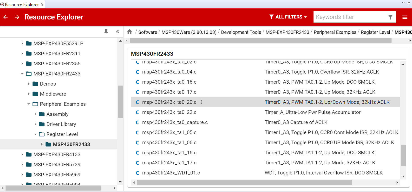
- Click import in the upper right hand corner
- Program the launchpad
Up/Down Mode Code Review
Looking at the main function in this example code, it only configures two modules:firth the GPIO, then the timerA0. Compared to the first task, we are not configuring the MSP430 clock system. So we are using the default setting of the clock system.
    //******************************************************************************
    // Main ************************************************************************
    // Configure the P1.1 and P1.2 as PWM signal output. Then configure timerA0    *
    // in Up/Dowm mode                                                             *
    //******************************************************************************

    int main {
        WDTCTL = WDTPW | WDTHOLD;                  // Stop WDT
        P1DIR |= BIT1 | BIT2;                      // P1.1 and P1.2 output
        P1SEL1 |= BIT1 | BIT2;                     // P1.1 and P1.2 options select

        // Disable the GPIO power-on default high-impedance mode to activate
        // previously configured port settings
        PM5CTL0 &= ~LOCKLPM5;

        TA0CCR0 = 128;                             // PWM Period/2
        TA0CCTL1 = OUTMOD_6;                       // TACCR1 toggle/set
        TA0CCR1 = 32;                              // TACCR1 PWM duty cycle
        TA0CCTL2 = OUTMOD_6;                       // TACCR2 toggle/set
        TA0CCR2 = 96;                              // TACCR2 PWM duty cycle
        TA0CTL = TASSEL_1 | MC_3;                  // ACLK, up-down mode

        __bis_SR_register(LPM3_bits);              // Enter LPM3

        return 0;
    }
main()
Configure the GPIO settings. Set the P1.1 and P1.2 as the PWM output pins. Be awared, we are not using an external crystal in this task. So no need to configure the XT1 here.
    P1DIR |= BIT1 | BIT2;                             // P1.1 and P1.2 output
    P1SEL1 |= BIT1 | BIT2;                            // P1.1 and P1.2 options select
PWM signal output pin setting
Now we start to configure the timer. The timerA0 is using ACLK as the clock source.
What is the default ACLK frequency? (Hint: Check the user's guide and datasheet)
The ACLK is using REFO as clock source. The REFO should be around 32768Hz as default. See the device specific data sheet for more detail information about the REFO. If you are looking for generating a high precision PWM signal, we would recommend you to use an external crystal as the timer clock source, like we do in Task 1.
The timer output mode will also impact the output signal. Different timer output mode in Up/Down mode shows below.
In this example, we are using Up/Down mode with Toggle/Set output mode to generate the PWM signals. Set ACLK as the timerA0 clock source. Set timerA0 as Up/Down mode. Set the TA0CCR1 and TA0CCR2 output mode as Toggle/Set mode and configure the PWM duty.
    TA0CCR0 = 128;                             // PWM Period/2
    TA0CCTL1 = OUTMOD_6;                       // TACCR1 toggle/set
    TA0CCR1 = 32;                              // TACCR1 PWM duty cycle
    TA0CCTL2 = OUTMOD_6;                       // TACCR2 toggle/set
    TA0CCR2 = 96;                              // TACCR2 PWM duty cycle
    TA0CTL = TASSEL_1 | MC_3;                  // ACLK, up-down mode
configure PWM output
Up/Down Mode Logic Captures
Build and download the program to the launchpad. Use a Logic Probe to capture the P1.1 and P1.2 signals. Please think about the folowing two questions before checking the results.
What's the right answer here?
How to calculate the PWM frequency?
What is the duty of the P1.2 signal?
The capture shown here is the P1.1 and P1.2 output PWM signals.
Summary
At the end of this lab, you should now be able to:
- Understand the different timer operation modes
- Understand the different timer output modes
- Generate any PWM signals
This work is licensed under a Creative Commons Attribution-NonCommercial-NoDerivatives 4.0 International License.