Hardware Architecture
The CC13x2 or CC26x2
Arm Cortex-M4F (System Core)
The system core (CM4F) is designed to run the wireless protocol stack from the link layer up to the user application. The link layer interfaces to the radio core through a software module called the RF driver, which sits above the RF doorbell. The RF driver runs on the CM4F and acts as an interface to the radio on the CC13x2 or CC26x2, and also manages the power domains of the radio hardware and core. Documentation for the RF driver can be found at the TI Drivers API Reference.
Arm Cortex-M0 (Radio Core)
The Cortex-M0 (CM0) core within the CC13x2 or CC26x2 is responsible for both interfacing to the radio hardware, and translating complex instructions from the Cortex-M4F (CM4F) core into bits that are sent over the air using the radio. For Z-Stack, the CM0 implements the PHY layer of the protocol stack. Often, the CM0 is able to operate autonomously, which frees up the CM4F for higher-level protocol and application-layer processing.
The CM4F communicates with the CM0 through a hardware interface called the RF doorbell, which is documented in the CC13x2 CC26x2 SimpleLink Wireless MCU Technical Reference Manual. The radio core firmware is not intended to be used or modified by the application developer.
Flash, RAM, and Peripherals
The CC13x2x1 or CC26x2x1 contains 352 kB of in-system programmable flash memory and 80 kB of SRAM, whereas the CC13x2x7 or CC26x2x7 has 704 kB flash memory and 144 kB of SRAM. The flash is split into erasable pages of 8 kB. The CC13x2 or CC26x2 also contains 8 kB of cache SRAM that can be utilized to extend RAM capacity or can function as a normal cache to increase applicationperformance. The CC13x2 or CC26x2 also hosts a full range of peripherals including UART, I2C, I2S, AES, TRNG, temperature and battery monitors, 4x 32-bit timers, 2x SSI, and an integrated and autonomous sensor controller. See Sensor Controller for more information on the sensor controller.
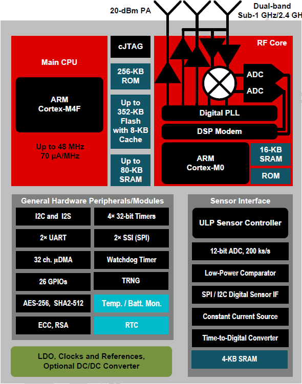
Figure 11. SimpleLink™ CC13x2x1 or CC26x2x1 Block Diagram
Note
As compared to the Block Diagram of the CC13x2x1 or CC26x2x1 shown above, CC13x2x7 or CC26x2x7 will have 704 kB of Flash and 144 kB of SRAM.
The CC13x1x or CC26x1x are cost-optimized devices with a reduced feature set, as such the following changes have taken effect:
- Features and peripherals which have been removed
- IEEE 754-compliant single-precision Floating Point Unit (FPU)
- Memory Protection Unit (MPU)
- AES 256-bit crypto accelerator
- ECC and RSA Public Key Hardware Accelerator
- SHA2 Accelerator
- Sensor Controller with 4KB of SRAM
- Further peripheral modifications
- 1x UART
- 1x SSI (SPI, MICROWIRE, TI)
- 32KB + 8KB GP cache SRAM, parity removed
- 40 KB ROM
Note
One implication of SRAM reduction is that Dynamic Multiprotocol Management (DMM) will not be possible for common use cases with CC13x1x or CC26x1x devices.
Programming Internal Flash With the ROM Bootloader
The CC13x2 or CC26x2 internal flash memory can be programmed using the bootloader located in device ROM. Both UART and SPI protocols are supported. See chapter 8 of the CC13x2 CC26x2 SimpleLink Wireless MCU Technical Reference Manual for more details on the programming protocol and requirements.
Note
Because the ROM bootloader uses predefined DIO pins for internal flash programming, allocate these pins in the board layout. The CC13x2 CC26x2 SimpleLink Wireless MCU Technical Reference Manual has more details on the pins allocated to the bootloader based on the chip package type.
Startup Sequence
For a complete description of the CC13x2 or CC26x2 reset sequence, see the CC13x2 CC26x2 SimpleLink Wireless MCU Technical Reference Manual.
Resets
Reset the device using only hard resets. From the software, this reset can be accomplished using:
HAL_SYSTEM_RESET();
In CCS, select Board Reset (automatic) from the reset menu (see Figure 12.).
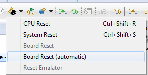
Figure 12. Board Reset