Multi-Channel Pulse-Width Modulation (MCPWM)
20 min read
The AM13x MCPWM page is currently in development for a later AM13x Academy release.
Overview
The C2000 high-performance control peripherals are an integral component for all digital control systems. This module covers the Multi-Channel Pulse Width Modulation (MCPWM) control peripheral.
What is pulse width modulation?
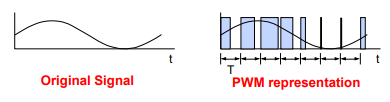
Pulse width modulation (PWM) is a general method for representing an analog signal with a digital approximation. A PWM signal consists of a sequence of variable width, constant amplitude pulses which contain the same total energy as the original analog signal.
This property is valuable in digital motor control as sinusoidal current (energy) can be delivered to the motor using PWM signals applied to a power converter. Although energy is input to the motor in discrete packets using PWM, the mechanical inertia of the rotor acts as a smoothing filter. Dynamic motor motion is therefore similar to having applied the sinusoidal currents directly.
PWM is a scheme to represent a signal as a sequence of pulses with the following characteristics: * Fixed carrier frequency * Fixed pulse amplitude * Pulse width that is proportional to instantaneous signal amplitude * PWM energy ~ original signal energy
Why use PWM with power-switching devices?
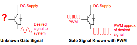
Power switching devices can be difficult to control when operating in the proportional region, but are easy to control in the saturation and cutoff regions. Since PWM is a digital signal by nature and easy for an MCU to generate, it is ideal for use with power switching devices. Essentially, PWM performs a DAC function, where the duty cycle is equivalent to the DAC analog amplitude value.
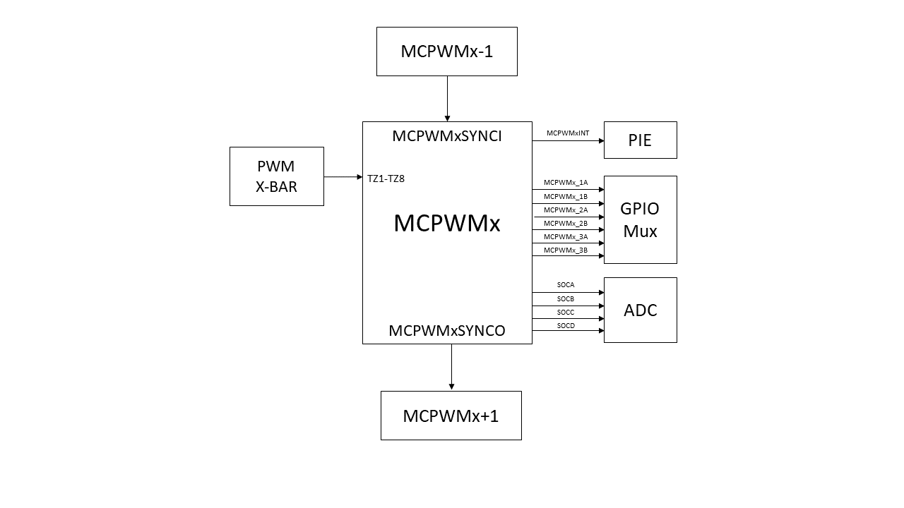
The MCPWM Module
MCPWM modules are highly programmable, extremely flexible, and easy to use, while being capable of generating complex pulse width waveforms with minimal CPU overhead or intervention. Each MCPWM module can have either 6 or 2 outputs, representing either 3 or 1 output pair(s). The names of the outputs are as follows:
MCPWM_1A
MCPWM_1B
MCPWM_2A (not applicable on 2-channel MCPWM)
MCPWM_2B (not applicable on 2-channel MCPWM)
MCPWM_3A (not applicable on 2-channel MCPWM)
MCPWM_3B (not applicable on 2-channel MCPWM)
Multiple MCPWM modules can be synchronized to operate together as needed within a system (please refer to your device’s documentation on the specific order of the MCPWM module synchronization scheme). The generated PWM waveforms are available as outputs on GPIO pins on the microcontroller.
The MCPWM module can also interact closely with other peripherals. For example, MCPWM’s can trigger ADC start-of-conversion (SOC) signals, and MCPWM’s can generate interrupts to the interrupt controller block. External signals can also be used to trip MCPWM outputs. Additionally, the outputs of comparators on the device can be used as inputs to the MCPWM by leveraging connectivity through the PWM X-BAR module.
MCPWM Submodules
Each MCPWM module consists of six main submodules:
Time-Base
Counter-Compare
Action-Qualifier
Dead-Band Generator
Trip-Zone
Event-Trigger
We will now go over the function and purpose of each submodule.
MCPWM Time-Base Submodule
The time-base submodule primarily consists of a 16-bit counter, along with built-in synchronization logic to allow multiple MCPWM modules to work together as a single system.
Clocking
The clock used for the MCPWM counter is originally sourced from a device’s system clock. MCPWM clock pre-scaler values can then be used to further divide down the system clock for the MCPWM counter and a MCPWM time-base period register. The counter and the time-base period value control the frequency and period of the generated MCPWM waveforms.
Pre-scaler Calculations:
Time-Base Clock
TBCLK= SYSCLK / (CLKDIV)Clock Pre-scaler = CLKDIV
Shadow Registers
Many MCPWM registers, such as the time-base period register, also have shadow registers. Shadow registers act like a buffer to allow register updates to be synchronized with the MCPWM counter or a specific (configurable) event and avoid corruption or spurious operation from the register being modified asynchronously by software. Unlike EPWM, the shadow registers on MCPWM have separate memory-mapped addresses, allowing the user to write directly to the shadow or active register as needed. Note that writes to the active register are blocked they are configured to get loaded by shadow register values. Refer to your device-specific technical reference manual to see the shadow load events for each register.
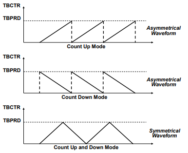
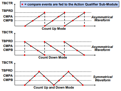
The time-base counter can operate in one of two modes:up-count, or up-down-count. Note that the up-count mode is used to generate asymmetrical waveforms, and the up-down-count mode is used to generate symmetrical waveforms.
Up-Count Mode
The counter starts counting from zero and increments until it reaches the time-base period register value, then the counter resets to zero and the count sequence starts again.
Up-Down-Count Mode
The counter starts counting from zero and increments until it reaches the time-base period register value, then the counter decrements until it reaches zero and the count sequence repeats.
Synchronization
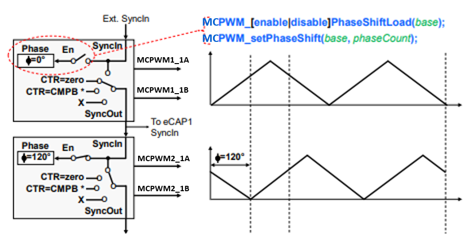
Synchronization allows multiple MCPWM modules to work together as a single system. The synchronization is based on an input signal called the SYNC-IN signal. Additionally, the waveform can be phase-shifted or offset as seen in the figure below.
MCPWM Counter-Compare Submodule
The counter-compare submodule continuously compares the time-base counter value to its counter-compare register values (PWMx_CMPA, PWMx_CMPB, CMPC, CMPD) and recognizes if the time-base counter matches a counter-compare value.
Compare Events
When a match occurs (counter = CMPx), this is known as a compare event. Compare events are used by the MCPWM action-qualifier and event-trigger submodules to influence MCPWM outputs and interact with other peripherals. The below MCPWM Counter-Compare Event Waveform diagram shows compare matches that are used by the action-qualifier submodule. Note that for up-count and down-count modes, a counter-compare match (counter = CMPx) can occur only once per cycle; however, for up-down-count mode, a counter match can occur twice per cycle since there can be a match on the up-count and another match on the down-count.
Shadowing
The counter compare registers also have shadow registers (PWMy_CMPxS, CMPxS) to help prevent corruption or glitches during the active PWM cycles. When configuring shadow load events to load the value in the shadow register to the active register, the user must write to the shadow register in their code.
MCPWM Action-Qualifier Submodule
The action-qualifier submodule is responsible for constructing the shape of PWM waveforms. This submodule utilizes compare events from the time-base and counter-compare submodules (above) to performing actions on an MCPWM modules output channels. These first three submodules (time-base, counter-compare, and action-qualifier) are the key submodules needed to generate basic PWM waveforms.
Action-Qualifier Actions
The action-qualifier submodule can perform the following actions on an MCPWM signal:
Set PWM output high
Clear PWM output low
Toggle PWM output (if high, toggle low; if low, toggle high)
Do nothing to PWM output
These actions are performed when a specific (configurable) event occurs as demonstrated in the table below.
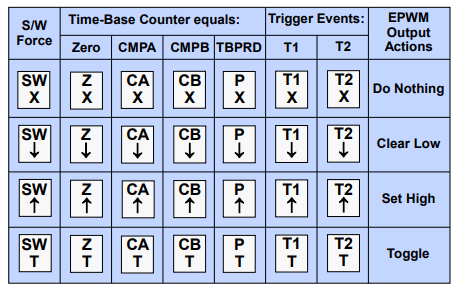
A match event can occur when the time-base counter is equal to the time-base period value, the time-base counter is equal to zero, the time-base counter equals CMPA, or the time-base counter equals CMPB. These event actions can also be specific to the counting direction of the time-base counter (counting up versus counting down).
Note that zero and time-base period match events are fixed in time, whereas CMPA and CMPB actions can be adjusted in times by programming the CMPA and CMPB registers values. Actions are configured independently for each MCPWM channel’s output using shadowed registers, and any or all events can be configured to generate actions on either channel’s output. Additionally, an action on any MCPWM output can be forced using software.
Action-Qualifier Examples
The below figures showcase how the action-qualifier module can be used with the compare match events to construct MCPWM waveforms. Note that there are up to 3 instances of channel pairs such as those depicted below on a single MCPWM module instance.
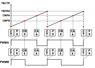
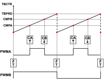
In the figure above, the PWMA output is set high on a zero match and cleared low on a compare A (CMPA) match. The PWMB output is set high on a zero match and cleared low on a compare B (CMPB) match.
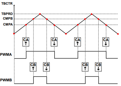
In the figure above, the PWMA output is set high on a compare A (CMPA) match and cleared low on a compare B (CMPB) match, while the PWMB output is toggled on a zero match.
In the figure above, there are now different output actions on the up-count and down-count using a single counter-compare register. The PWMA and PWMB outputs are set high on a compare A and B up-count match (CMPAU and CMPBU) and cleared low on a compare A and B down-count match (CMPAD and CMPBD).
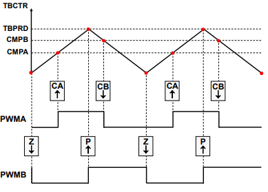
In the final figure above, there are again different output actions used on the up-count and down-count, the PWMA output is set high on a compare A up-count match (CMPAU) and cleared low on a compare B down-count match (CMPBD). The PWMB output is cleared low on a zero match and set high on a time-base period match.
MCPWM Waveform Generation
There are several important parameters that must be accounted for when generating a PWM waveform for your application. This includes PWM frequency, duty cycle, and resolution.
Switching Frequency
The PWM frequency (also called the carrier frequency) is determined by the time-base period value and the frequency of the MCPWM clock. To determine your time-base period value, use the below calculations. Recall that up-count and down-count modes produce asymmetric PWMs while up-down-count produces a symmetric PWM.
Asymmetric PWM
Time-Base Period = (Tpwm / TTBCLK) - 1
Tpwm = switching period
TTBCLK = timer period
Symmetric PWM
Time-Base Period = Tpwm / (2 * TTBCLK)
Tpwm = switching period
TTBCLK = timer period
Notice that in the symmetric case, the period value is about half that of the asymmetric case. This is because for up-down-count mode, the timer period is twice the value specified in the time-base period register (i.e. the timer counts up to the period register value and then counts back down).
Duty Cycle
The duty cycle is typically a percentage value that describes how long a PWM output is high (also referred to as on-time) For example, a 50% duty cycle indicates the PWM is high (on) for 50% of a period and low (off) for 50% of a period. In simple PWM waveforms, a PWM output will typically start in a low state and be set high on a counter-compare match event. In this case, duty cycle calculations are used to determine what counter-compare value is needed. The counter-compare value can be calculated as follows: Asymmetric PWM
CMPx= (100% - duty cycle)∗TBPRDSymmetric PWMCMPx= (100% - duty cycle)∗TBPRDNote that for symmetric PWM, the desired duty cycle is only achieved if the compare registers contain the computed value for both the up-count compare and down-count compare portions of the time-base period.
Resolution
The resolution of a PWM signal can be calculated after the time-base period register value is determined. The function resolution uses the largest power of 2 that is less than (or close to) the time-base period value. Examples are listed below: Asymmetric PWM
Asymmetric PWM time-base period value = 1000
This PWM has approximately 10-bit resolution since 2^10 = 1024 (this is approximately equal to 1000) Symmetric PWM
Symmetric time-base period value was 500
This PWM has approximately 9-bit resolution since 2^9 = 512 (this is approximately equal to 500)
MCPWM Calculations Examples
Determine the time-base period (TBPRD) and counter-compare A (PWMx_CMPA) values needed to produce the following MCPWM signal (assuming TBCLK = 100MHz):
Frequency = 100kHz
Duty cycle = 25%
Symmetric PWM Calculations
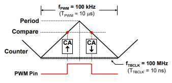
TBPRD = .5 * (FTBCLK/FPWM) = .5 * (100 MHz / 100 kHz) = 500
CMPA = (100% - duty cycle) TBPRD = 0.75 * 500 = 375
Asymmetric PWM Calculations
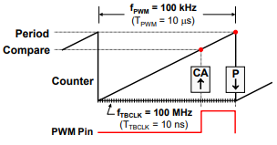
TBPRD = (FTBCLK/FPWM) - 1 = (100 MHz / 100 kHz) - 1 = 999
CMPA = (100% - duty cycle) (TBPRD +1) - 1 = 0.75 * (999 + 1) - 1 = 749
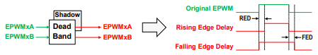
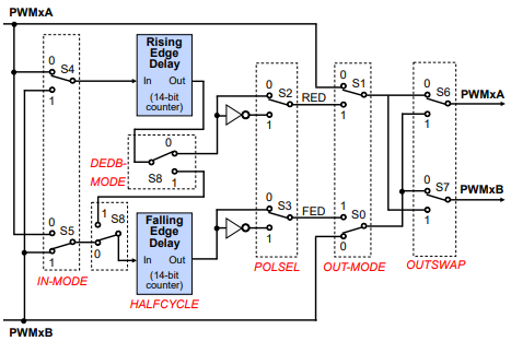
MCPWM Dead-Band Submodule
The dead-band submodule provides a way to delay the switching of the PWM (high to low or low to high). By delaying the transition of PWM signals, you can allow time for the PWM gates to turn off and prevent a short circuit. We will refer to the PWM switching in terms of rising edges (low to high) and falling edges (high to low).
The dead-band submodule supports independently programmable rising-edge and falling-edge delays with various options for generating the appropriate signal outputs on MCPWMx_yA and MCPWMx_yB. For each MCPWM module, the dead-band configurations are shared across all A-channels and all B-channels. For example, MCPWMx_1A cannot have separate dead-band configurations from MCPWMx_2A and MCPWMx_3A, etc.
Why use Dead-Band?
PWM outputs switch by flipping transistor gates on and off. However, transistor gates turn on faster than they shut off! If two gates are on at the same time (even momentarily), this produces a path from supply rail to ground and yields a short circuit. The dead-band submodule can alleviate this issue.
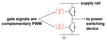
Dead-band control provides a convenient means of combating current shoot-through problems in a power converter. Shoot-through occurs when both the upper and lower gates in the same phase of a power converter are open simultaneously (both gates “on”). This condition shorts the power supply and results in a large current draw. Shoot-through problems occur because transistors open faster than they close, and because high-side and low-side power converter gates are typically switched in a complimentary fashion. Although the duration of the shoot-through current path is finite during PWM cycling, (i.e. the closing gate will eventually shut), even brief periods of a short circuit condition can produce excessive heating and over stress the power converter and power supply.
Preventing Short-Circuits
There are two basic approaches exist for controlling shoot-through:
Modify the transistors
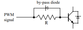
The opening time of the transistor gate must be increased so that it (slightly) exceeds the closing time. One way to accomplish this is by adding a cluster of passive components such as resistors and diodes in series with the transistor gate, as shown in the image below.
The resistor acts to limit the current rise rate towards the gate during transistor opening, thus increasing the opening time. When closing the transistor however, current flows unimpeded from the gate via the by-pass diode and closing time is therefore not affected. While this passive approach offers an inexpensive solution that is independent of the control microprocessor, it is imprecise, the component parameters must be individually tailored to the power converter, and it cannot adapt to changing system conditions.
Modify the PWM gate signals controlling the transistors
This approach separates transitions on complimentary PWM signals with a fixed period of time. This is called dead-band. While it is possible to perform software implementation of dead-band, the C2000 MCUs offer on-chip hardware for this purpose that requires no additional CPU overhead. Compared to the passive approach, dead-band offers more precise control of gate timing requirements. In addition, the dead time is typically specified with a single program variable that is easily changed for different power converters or adapted on-line.
MCPWM Trip-Zone Submodule
The trip zone submodule provides a protection mechanism to protect the output pins from abnormalities, such as over-voltage, over-current, and excessive temperature rise.
Using the trip-zone is the quickest way to change a PWM output. The trip-zone submodule utilizes a fast, clock-independent logic mechanism to quickly handle fault conditions by forcing the MCPWMx_yA and MCPWMx_yB outputs to a safe, configurable state (such as high, low, or high-impedance). Due to its speed and hardware connection, the trip-zone can be used when interrupts (ISR software) may not be quick enough to protect the hardware in response to over-current conditions or short-circuits.
The trip-zone supports two types of trips
One-shot (OSHT) trips for major short circuits or over current conditions
Cycle-by-cycle (CBC) trips for current limiting operation
Trip-Zone Signals
Trip-zone signals (TZ1-TZ8) are all sourced from the PWM X-BAR module. Refer to your device-specific TRM to see the trip sources that can be fed to the PWM X-BAR outputs.
PWM X-BAR
The PWM X-BAR is used to route various internal and external signals to the MCPWM modules. Eight trip signals from the PWM X-BAR are routed to all of the MCPWM modules.
The PWM X-BAR architecture block diagram shown below is replicated 8 times. The PWM XBAR can select a single signal or logically OR up to 32 signals. The table in the figure defines the various trip sources that can be multiplexed to the trip-zone and digital compare submodules.
MCPWM Event-Trigger Submodule
The event-trigger submodule can use the events generated by the time-base, counter-compare, and trip-zone submodules to trigger two types of actions:
Generate an interrupt to the CPU
Generate a start-of-conversion (SOC) pulse to the ADC
The event-trigger submodule also incorporates pre-scaling logic to issue an interrupt request or ADC SOC on every event or up to every fifteenth event.
These event triggers can occur at a number of configurable time such as when the time-base counter equals zero, period, zero or period, or on the up-count or down-count match of a counter-compare value (CMPx). Notice counter-up and counter-down triggers are independent and separate.
MCPWM Code Example
  //Configure the count mode to be up-count
  MCPWM_setTimeBaseCounterMode(MCPWM1_BASE, MCPWM_COUNTER_MODE_UP);
  //Configure the TBPRD shadow register to be 100
  MCPWM_setTimeBasePeriodShadow(MCPWM1_BASE, 100);
  //Configure the CMPA shadow register to be 25 for a 25% duty cycle
  MCPWM_setCounterCompareShadowValue(MCPWM1_BASE, MCPWM_COUNTER_COMPARE_1A, 25);
  //Configure the PWM output to go high on the time-base = 0 event
  MCPWM_setActionQualifierActionShadow(MCPWM1_BASE, MCPWM_AQ_OUTPUT_1A, MCPWM_AQ_OUTPUT_HIGH, MCPWM_AQ_OUTPUT_ON_TIMEBASE_ZERO);
  //Configure the PWM output to go low on the time-base = CMPA event
  MCPWM_setActionQualifierActionShadow(MCPWM1_BASE, MCPWM_AQ_OUTPUT_1A, MCPWM_AQ_OUTPUT_LOW, MCPWM_AQ_OUTPUT_ON_TIMEBASE_UP_CMPA);
Feedback
Please provide any feedback you may have about the content within AM13x Academy to: AM13x_academy_feedback@list.ti.com