Direct Memory Access (DMA) Lab#
The objective of this lab is to use the Direct Memory Access (DMA) controller to regularly service the ADC in a real-time data processing application. By using the DMA to move data, the CPU is saving instruction cycles that could be used on other critical tasks. Specifically, we will be using the PWM and ADC modules to generate and sample a PWM waveform at a chosen sampling rate. The DMA will then be used to store the ADC samples in a ping pong buffer, so groups of samples can simultaneously be processed by the CPU in an interrupt service routine (ISR). In addition to reviewing basics for the PWM and ADC modules, this lab should inform readers of how and why the DMA can be used to reduce load on the CPU.
Note:
This lab uses a Pulse Width Modulator (PWM). If using the LAUNCHXL_F28E12X,
the PWM module on this device is called the Multi-Channel Pulse Width Modulator (MCPWM);
follow the directions under the “Configure MCPWM” section. For all other devices, the PWM module
is called the Enhanced Pulse Width Modulator (ePWM); follow the directions under the “Configure ePWM” section.
This lab cannot be performed on the following devices since there is no DMA module:
F280013x
F280015x
Solution#
All C2000 Academy lab software solutions are located in the directory: [C2000Ware_Install_Path]/training/device/[device_name].
Overview#
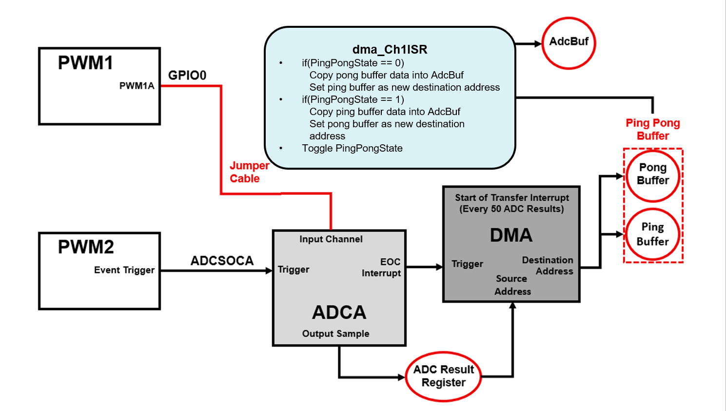
In this lab, we will use the Sysconfig GUI to generate a waveform with one of the PWM modules, like the ePWM & MCPWM labs. Also, similar to the ePWM & MCPWM lab, the ADC will be setup to sample the PWM waveform at a chosen sampling rate. At the end of each conversion, however, the ADC will trigger the DMA rather than triggering an interrupt on the CPU.
The first time that the DMA is triggered will be the start of the first ‘Transfer’. Since we will have configured our DMA to generate an interrupt at the start of ‘Transfers’, the DMA will immediately trigger an interrupt before the first ‘Burst’ is sent. This very first interrupt should set the DMA destination address to the Ping Buffer, while the CPU copies the contents of the still empty Pong Buffer into a buffer called AdcBuf. During the next interrupt, the destination address of the DMA will change to the Pong Buffer, while the CPU copies from the Ping Buffer. Because we set the ‘Transfer’ size of the DMA to be 50 ‘Bursts’, the DMA interrupt will be triggered on every 50th ADC conversion before the first ‘Burst’ of the ‘Transfer’. You can see the details of the interrupt in the dma_Ch1ISR code block included later in the lab.
You will be able to view the contents of any of these buffers in Code Composer Studio (CCS). In this application, the DMA allows the CPU to reclaim instruction cycles that would have been necessary to continuously copy data from the ADC registers into memory, which allows for more instruction cycles to be allocated for other tasks.
Lab Setup#
Hardware Setup#
Required hardware for this lab:
A C2000 controlCARD or LaunchPad with the supplied USB cable.
Jumper cables (1).
Oscilloscope (optional). Using the supplied USB cable, connect the USB Micro or Mini Type-B connector into your C2000 board and the USB Standard Type-A connector into your computer’s USB port (please note that controlCARD docking stations may require an additional power supply connection). You should see some LEDs light up on the board. This connection will power the board and provide a JTAG communication link between your device and CCS. Refer to Getting Started module for more details if needed.
Later in the lab we will be routing the output pin of the PWM waveform to the input pin of the ADC, so make sure that you have enough jumper cables to facilitate this.
Software Setup#
Required computer software installation for this lab:s
Start a CCS Project#
Our first task is to import an empty project to our Code Composer Studio (CCS) workspace. The basic instructions are as follows:
Open CCS and go to Project→Import CCS Projects. A new window should appear. Ensure that the Select search-directory option is activated.
Click the Browse button and select the
[C20000ware_Install_dir]/training/device/[device]/empty_labdirectory. Note that the default Windows [C20000ware_Install_dir] isC:/ti/c2000/C2000Ware_x_xx_xx_xx.Under Discovered Projects, you should now see the
lab_[board]_[device]project. Select the appropriate project for either the control card or the launchpad.
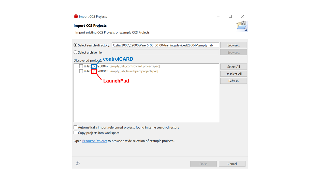
Click Finish to import and copy the
lab_[board]_[device]project into your workspace.After the project has been imported, the project explorer window should look like below:

Rename the project to your liking
Right-click on the project in “Project Explorer” pane. Select ‘Rename’ from the drop down menu and rename the project to ‘c2000_dma_lab’ or a name of your choosing.
Now click the ‘Down Arrow’ located to the left of the imported project to expand it and select lab_main.c. Right-click on the file, and select ‘Rename’ to rename the file to c2000_dma_lab_main.c or a name of your choosing.
Configure the GPIO#
We will now start to configure the necessary GPIO pins. First, we will configure one of the board LEDs as an indicator.
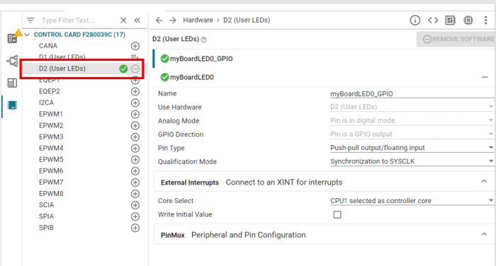
In the project, open the
.syscfgfile by double-clicking it.Navigate to the “Hardware” tab in Sysconfig
Click ‘+’ next to ‘LED’ to add an LED (it should be LED4/LED5 if using a LaunchPad, or D1/D2 if using a controlCARD)
Configure the PWMs#
Next, we will configure two PWMs. The first PWM waveform will be the output of ePWM1/MCPWM1 that will be used as an input to the ADC. The second PWM (ePWM2/MCPWM3) will be used to trigger an SOC on the ADC at a specified rate. For more information on the PWM and MCPWM, please review the Enhanced Pulse Width Modulation (EPWM) and Multi-Channel Pulse Width Modulation pages in the Control Peripherals module folder. View the table below to see which PWM module is present on your device, and what the corresponding PWM frequency will be for PWM1 depending on the device SYSCLK. Follow the corresponding directions (either “Configure ePWM” or “Configure MCPWM”).
Device |
PWM Module |
SYSCLK Frequency |
PWMCLK Frequency |
PWM1 Signal Frequency |
PWM2 Signal Frequency |
|---|---|---|---|---|---|
F28379D |
ePWM |
200 MHz |
100 MHz |
2 kHz |
50 kHz |
F2838x |
ePWM |
200 MHz |
100 MHz |
2 kHz |
50 kHz |
F28004x |
ePWM |
100 MHz |
100 MHz |
2 kHz |
50 kHz |
F28002x |
ePWM |
100 MHz |
100 MHz |
2 kHz |
50 kHz |
F28003x |
ePWM |
120 MHz |
120 MHz |
2.4 kHz |
60 kHz |
F28P65x |
ePWM |
200 MHz |
200 MHz |
4 kHz |
100 kHz |
F28P55x |
ePWM |
150 MHz |
150 MHz |
3 kHz |
75 kHz |
F28E12x |
MCPWM |
160 MHz |
160 MHz |
3.2 kHz |
80 kHz |
Note:
As is reflected in the above table, for Devices F2837xD, F2837xS, F2838x, F28003x, F28P65x, F28P55x and F28E12x:
The SYSCLK generated from the internal oscillator is higher than 100MHz on these devices. For example, the EPWM clock for F28003x is 120MHz. The maximum EPWM clock is still 100MHz on F2837xD, F2837xS, and F2838x, but the ADC clock is equal to the device SYSCLK. When clock dividers are selected in the following modules, you may need to modify your dividers to achieve exactly the same results. You may also notice that your device has different parameters than the ones seen in the images below. Do not worry, as all of the essential parameters for this lab are available on all devices.
Configure the MCPWM#
Note:
This section is only applicable to the F28E12x device. If using any other C2000 device, follow instructions in “Configure the ePWM” instead.
Set Up MCPWM1#
You may notice that the next sections are very similar to the MCPWM lab, but be careful, as the ADC configuration is slightly different. The code below configures MCPWM1A to output a PWM waveform with a 25% duty cycle. The desired MCPWM1 frequency for device’s with a 100 MHz SYSCLK frequency is 2kHz. C2000 devices with a SYSCLK frequency other than 100 MHz will have a different resulting PWM signal frequency (see the table in “Configure the PWMs”). This PWM waveform will be generated on a GPIO pin and used as a data input source to the ADC. For this, we will need to modify the configurations for the ‘MCPWM Time Base’, ‘MCPWM Counter Compare’, ‘MCPWM Action Qualifier’ and ‘PinMux’ subodules.
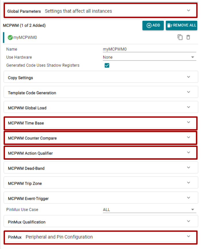
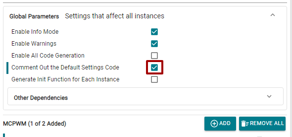
First, we will configure the MCPWM ‘Global Parameters’ to comment out all default code that configures a default setting to conserve memory on the device:
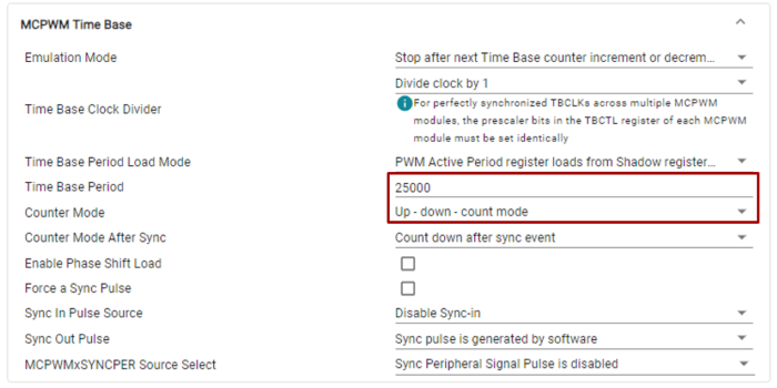
Second, we will configure the MCPWM1A to output a symmetrical PWM waveform, that is, configure the time base counter in up-down-count mode. Given that we are in up-down-count mode, and we want our PWM waveform to have a frequency of 2kHz, we have:
\(\text{Time Base Period}=\frac{f_{tbclk}}{2f_{pwm}}=\frac{100* 10^6}{2* 2000}=25000.\)
Configure the ‘MCPWM Time Base’ submodule as follows:
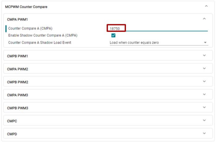
Next, we calculate the necessary counter compare value to achieve the desired duty cycle. Since we are in up-down-count mode and want our PWM waveform to have a 25% duty cycle, we have:
\(\text{Counter Compare Value}=(1-\frac{duty}{100})*tbprd=(1-\frac{25}{100})*25000=18750.\)
Configure the ‘MCPWM Counter Compare’ submodule for the CMPA of PWM1 as follows:
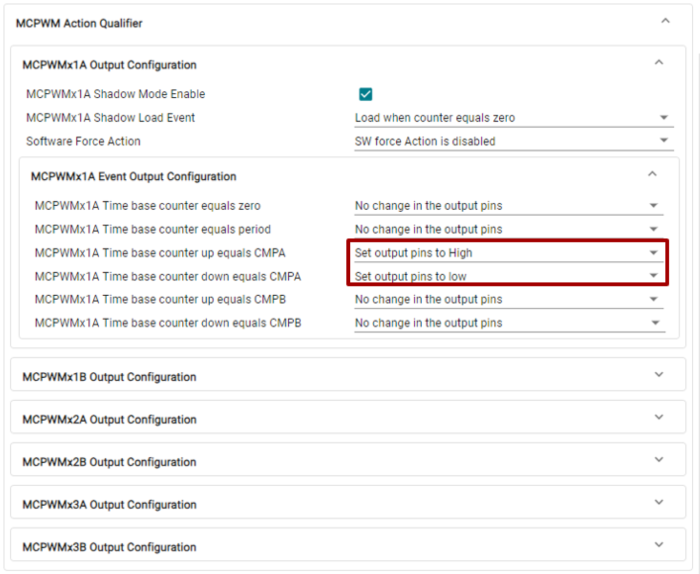
Lastly, configure the ‘MCPWM Action Qualifier’ submodule for the CMPA of PWM1 to force the output high on a count up event and low on a count down event:
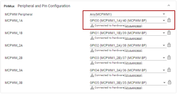
Make sure the ‘PinMux’ submodule is set to use MCPWM1 and (optionally) modify the MCPWM_1A GPIO to an unused GPIO on the controlCARD or LaunchPAD:
This results in the desired PWM waveform.
Set Up MCPWM3#
We will use a second PWM module to sample the ADC. The desired PWM frequency for device’s with a 100 MHz SYSCLK frequency is 50kHz. C2000 devices with a SYSCLK frequency other than 100 MHz will have a different resulting PWM signal frequency (see the table in “Configure the PWMs”). Note that some devices (F28E12x for example) do not have a MCPWM2, so we are using MCPWM3. For this PWM, the only Sysconfig submodules we will need to modify are ‘Global Parameters’, ‘MCPWM Time Base’, ‘MCPWM Event Trigger’, and ‘PinMux’. Since the MCPWM SOC and ADC SOC connection is internal to the device, we don’t need to configure the Pinmux GPIOs for MCPWM.
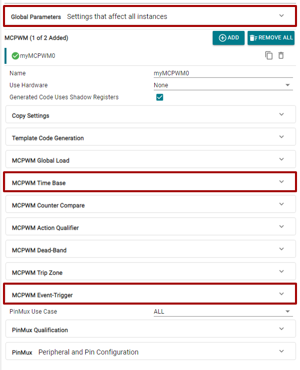
Click the ‘+’ icon next to MCPWM again to add a second MCPWM instance. First, we will configure the MCPWM ‘Global Parameters’ to comment out all default code that configures a default setting to conserve memory on the device:
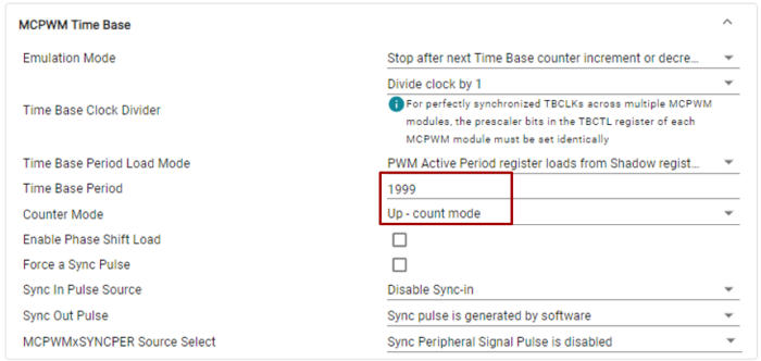
Unlike MCPWM1A, notice that MCPWM3 is setup to operate in up count mode, hence, we have:
\(\text{Time Base Period}=\frac{f_{tbclk}}{f_{pwm}}-1=\frac{100* 10^6}{50000}-1=1999.\)
Configure the ‘MCPWM Time Base’ submodule as follows:
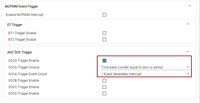
We will enable ADC SOC triggering with the MCPWM3 SOCA signal. Configure the “Event-Trigger’ submodule:
If MCPWM1 is selected in the ‘PinMux’, you will likely have an error in Sysconfig due to MCPWM1 also being configured for the previous instance. Make sure to set ‘MCPWM Peripheral’ to MCPWM3, if it is not already.
This concludes the configuration of the MCPWM modules. Skip over the ePWM section and configure the ADC next.
Configure the ePWM#
Note:
This section is only applicable to devices other than the F28E12x device. If using F28E12x, follow instructions in “Configure the MCPWM” instead.
Set Up ePWM1#
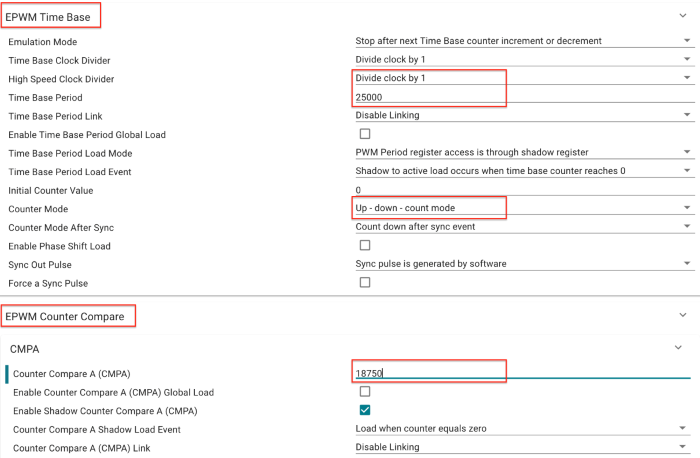
You may notice that the next sections are very similar to the ePWM lab, but be careful, as the ADC configuration is slightly different. The code below configures ePWM1A to output a PWM waveform with a 25% duty cycle. The desired PWM frequency for device’s with a 100 MHz SYSCLK frequency is 2kHz. C2000 devices with a SYSCLK frequency other than 100 MHz will have a different resulting PWM signal frequency (see the table in “Configure the PWMs”). This PWM waveform will be used as a data input source. Notice that ePWM1A is setup to output a symmetrical PWM waveform, that is, the time base counter is setup in up-down-count mode. Given that we are in up-down-count mode and we want our ePWM waveform to have a frequency of 2kHz, we have:
\(\text{Time Base Period}=\frac{f_{tbclk}}{2f_{pwm}}=\frac{100* 10^6}{2* 2000}=25000.\)
Next, we note the configuration of the duty cycle. Since we are in up-down-count mode and we want our PWM waveform to have a 25% duty cycle, we have:
\(\text{Counter Compare Value}=(1-\frac{duty}{100})*tbprd=(1-\frac{25}{100})*25000=18750.\)
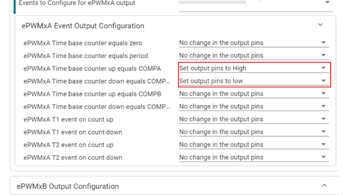
The action qualifier submodule is then set to force the output to be high on a count up event and low on a count down event. This results in the desired PWM waveform.
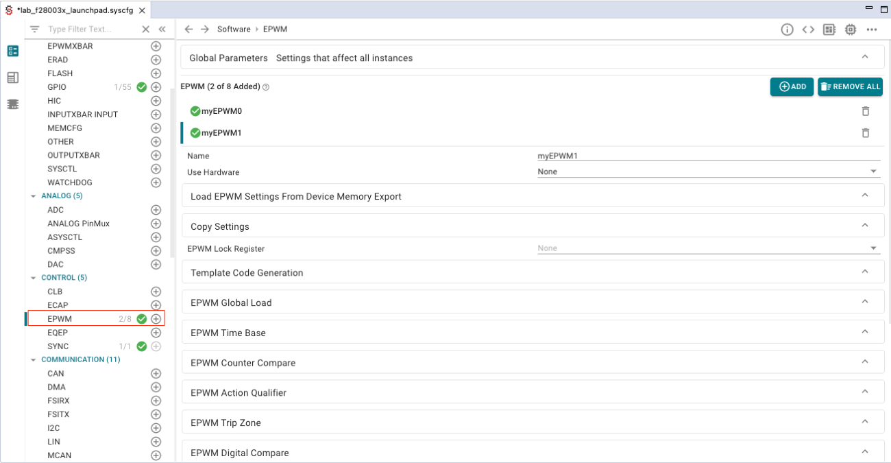
To implement the above described specifications for ePWM1 in SysConfig, first click the ‘+’ by EPWM in SysConfig to open an instance of the EPWM module.
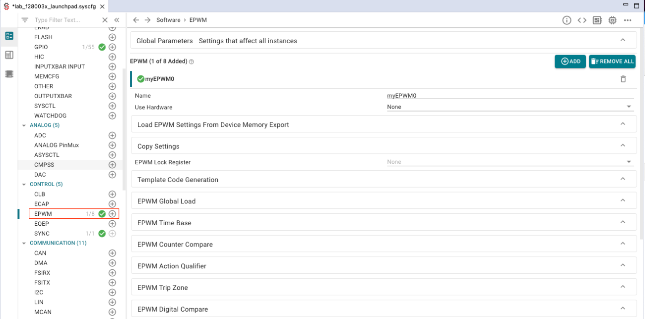
Expand the ‘EPWM Time Base’ dropdown menu, and apply the changes circled below.
Expand the ‘EPWM Counter Compare’ dropdown menu, and again apply the circled changes.
Expand the ‘ePWMxA Event Output Configuration’ dropdown menu, then apply the changes circled below.
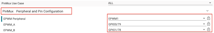
Expand the ‘PinMux Peripheral and Pin Configuration’ dropdown menu. For ‘EPWM Peripheral’, make sure to select instance EPWM1. Also, make sure to select ‘GPIO0’ for ‘EPWMA’ and select ‘GPIO1’ for ‘EPWMB’, as shown below. The pin number will vary based on hardware. The
Set Up ePWM2#
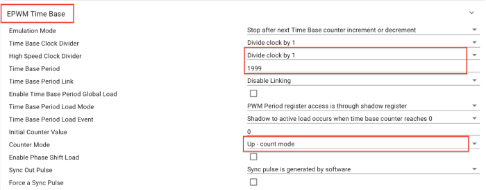
In this lab, the ADC will be used to sample the generated PWM waveform from ePWM1A. The desired PWM frequency for device’s with a 100 MHz SYSCLK frequency is 50kHz. C2000 devices with a SYSCLK frequency other than 100 MHz will have a different resulting PWM signal frequency (see the table in “Configure the PWMs”). The below code configures ePWM2 to trigger an SOC on the ADC at the specified frequency. Unlike ePWM1A, notice that ePWM2 is setup to operate in up count mode, hence, we have:
\(\text{Time Base Period}=\frac{f_{tbclk}}{f_{pwm}}-1=\frac{100* 10^6}{50000}-1=1999.\)
To implement the above described specifications for ePWM2 in SysConfig, click the ‘+’ by EPWM to open another instance of the EPWM module.
Expand the ‘EPWM Time Base’ dropdown menu, and apply the changes circled below.
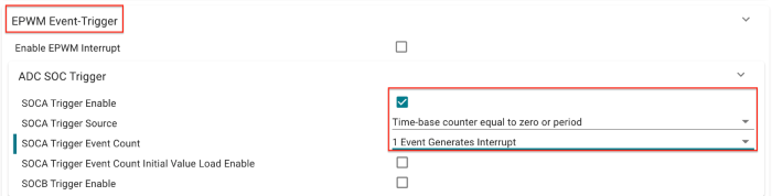
Expand the ‘EPWM Event-Trigger’ dropdown menu, and apply the changes circled below.
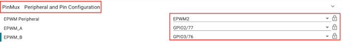
Expand the ‘PinMux Peripheral and Pin Configuration’ dropdown menu, and apply the changes circled below. Also, make sure to select ‘GPIO2’ for ‘EPWMA’ and select ‘GPIO3’ for ‘EPWMB’, as shown below. The pin number will vary based on hardware.
This concludes the configuration of the ePWM modules.
A more detailed explanation of the ePWM configuration
The configuration of both ePWM1A and ePWM2 above is identical to that of the lab in ePWM Lab, so you should see that lab for a more detailed explanation.
Configure the ADC#
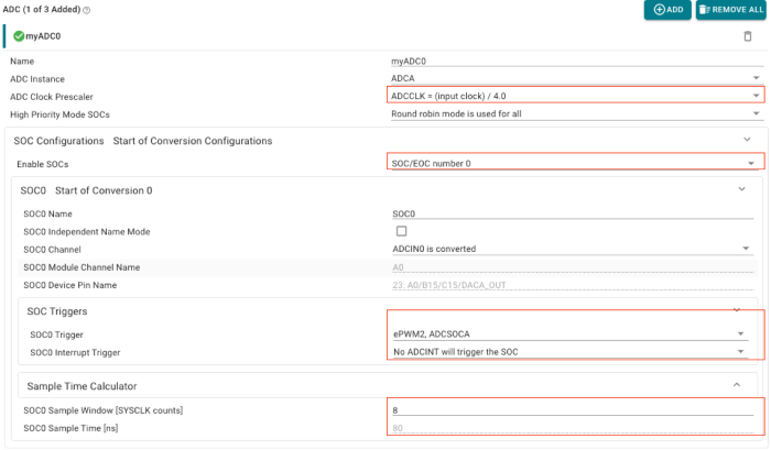
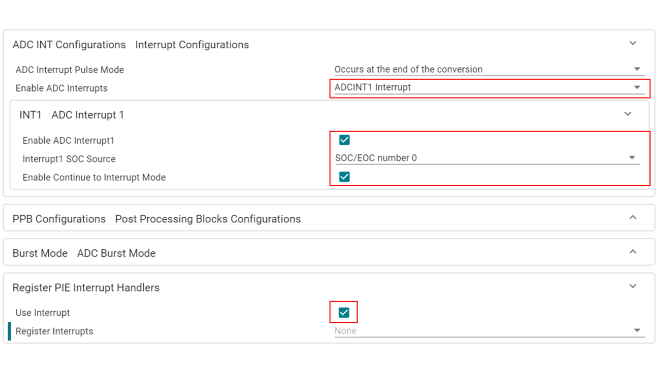
In the previous section, we explained that PWM2 (ePWM2/MCPWM3) would be triggering a SOC event on the ADC. In this section, we will provide the code to configure the ADC. More details about the configuration of the ADC can be found in the “Analog to Digital Converter (ADC) chapter under Analog Subsystem”. However, notice that we have setup a SOC to be triggered by PWM2. Next, we setup the ADC to interrupt at the end of a conversion. This interrupt will be utilized by the DMA so it knows when to load new samples from the ADC onto the ping pong buffer. The ADC is also setup in continuous mode so that the ADC register always contains the most recent sample.
Add ADC by clicking the ‘+’ by ADC in the SysConfig screen. Make sure to make the changes circled below. If your device SYSCLK is not 100MHz, you will need to change the ADC Clock Prescaler to acheive the same results.
For the ‘SOC0 Sample Window[SYSCLK counts]’ parameter, the same value may result in a different ‘SOC0 Sample Time[ns]’ on different devices, due to varying SYSCLK frequencies across devices. Make sure that the generated ‘SOC0 Sample Time[ns]’ is about 80ns.
Expand the ‘ADC INT Configurations’ dropdown menu, make the changes circled below.
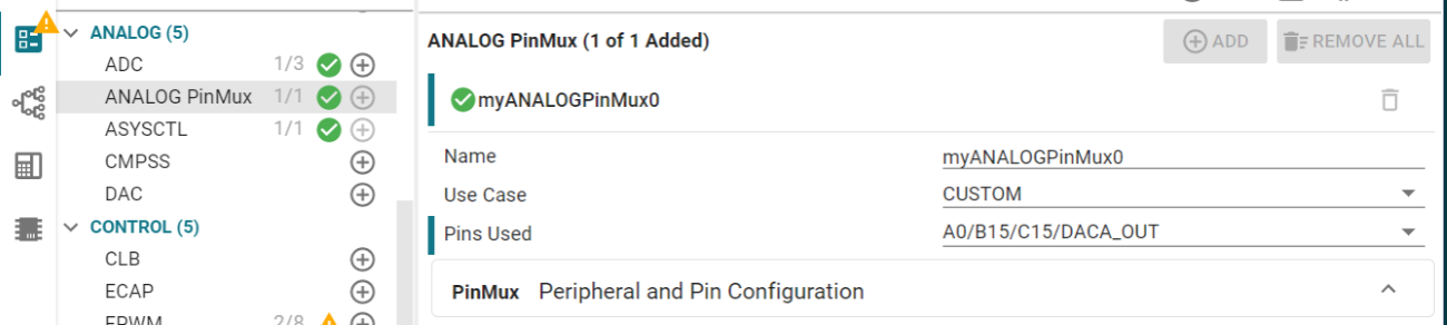
Navigate to the ANALOG PinMux tab and ensure the “Use Case” is set to “CUSTOM”.
Define the “Pins Used” to be the corresponding ADCINA0 pin (A0).
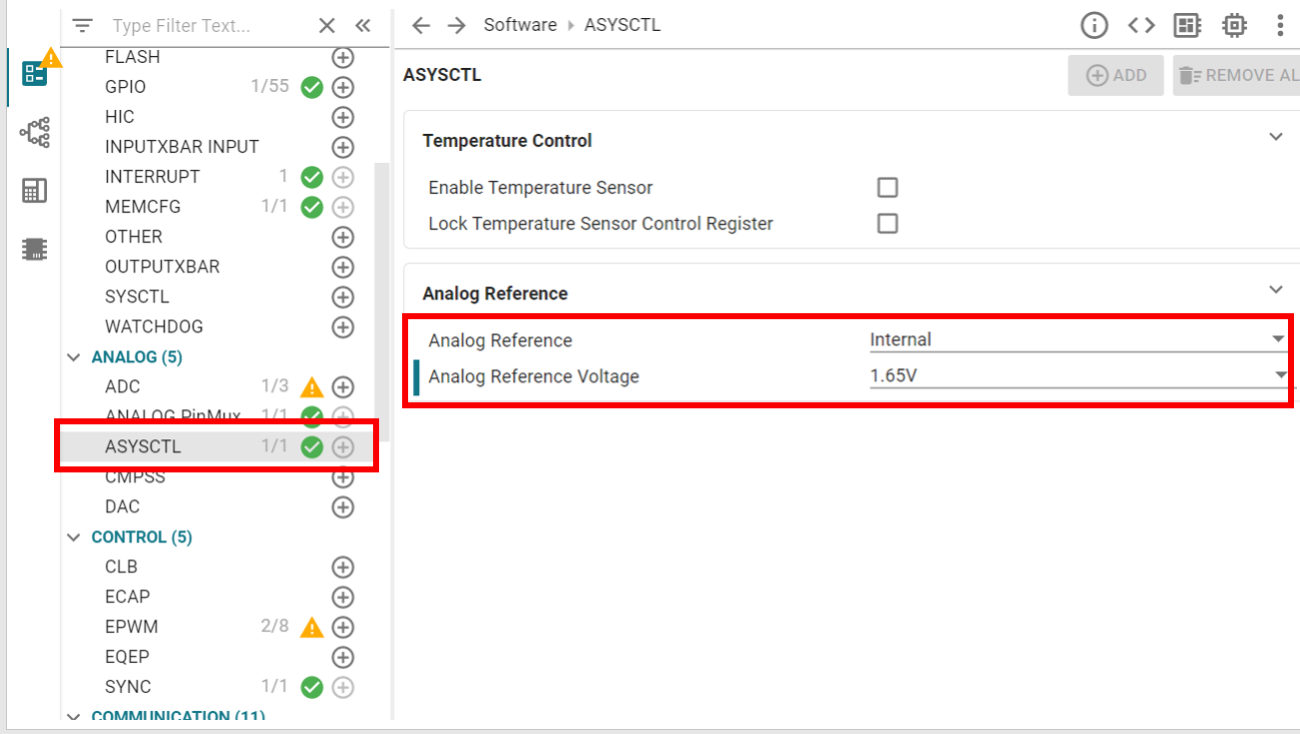
For devices F28002x, F28003x, F28004x, F28P65x, F28P55x, F28E12x:
Set analog reference voltage using asysctl parameter.
If the ADC module has already been added, select ASYSCTL in the ANALOG group and change the analog reference voltage to be an internal voltage of 1.65V. Otherwise, add ASYSCTL by clicking ‘+’ in ANALOG group and then add internal reference of 1.65V.
If using F28P65x LaunchPad, be sure to remove the external voltage reference jumper from your LaunchPad to generate the correct output signals for this lab.
Configure the DMA#
In this section, we will configure the DMA using the SysConfig GUI tool. We only need to configure one DMA channel: Channel 1. The trigger for DMA channel 1 is set to be from ADCA1, which signals to the DMA that a new sample is ready to be moved to the ping pong buffer. Notice that one-shot mode has been disabled and continuous mode has been enabled. Continuous mode ensures that the DMA is re-initialized after it completes a full transfer, which is needed to continuously retrieve samples from the ADC, otherwise, the DMA would halt and we would need to re-enable it in software each time. Additionally, notice that the word size is set to be 16 bits since the ADC result register is a 16-bit register.
Click
+next to DMA (in the COMMUNICATION Group) to add a DMA instance and select the below configurations for the top-level of the module::
The source and destination addresses will be used by the DMA to read data from and then write data to respectively. The source address will be the ADC result register since this is the only memory location we need the DMA to read from. Note that since the source address will always remain the same, the ‘Source Address Burst Step’ and ‘Source Address Transfer Step’ sizes are set to 0.
Expand the ‘Source Address Setup’ submodule and make the following modifications:
The DMA destination will ping pong between the ping buffer - the first 50 words in the AdcBufRaw array, and the pong buffer - the last 50 words in the AdcBufRaw array. We will initialize the DMA destination address to start at the beginning of the ping buffer. The DMA ISR will take care of switching the starting destination addresses between each 50 word transfer. The ‘Destination Address Transfer Step’ is set to 1 so that each time the DMA copies a burst of ADC data over to the buffer, the address it is placed at in the buffer is incremented by 1 each time.
Expand the ‘Destination Address Setup’ submodule and make the following modifications:
Now we will configure our DMA interrupt that we previously set up to occur at the start of each transfer.
Expand the ‘DMA Interrupt’ submodule and make the following modifications:
Ensure that the ISR name is dma_Ch1ISR since this will need to match the ISR name used in the main code.
This concludes the configuration of the DMA.
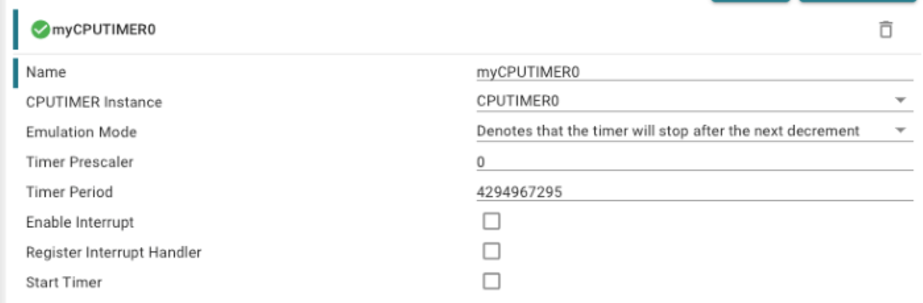
Configure the CPUTIMER#
In this section, we provide the code to setup CPUTIMER0. This timer will be
used to capture the runtime of the DMA ISR. It is important that the runtime of
the DMA ISR does not exceed the product of the ADC sampling period with
ADC_BUF_LEN because this implies that the DMA will start to overwrite the
contents of next buffer. Notice how the timer period is set to be the maximum
value of the 32-bit counter. The system clock will be driving this counter at a
frequency of DEVICE_SYSCLK_FREQ.
Click
+next to CPUTIMER (in SYSTEM Group) to add CPUTIMER instance
Program Setup#
Define Global Macros and Variables#
First, we will define some necessary macros and global variables, and we will
configure the destination and source address of the DMA transfer. The global
variable AdcBufRaw points to a ping pong buffer of size 2*50 and type
uint16_t. Accordingly, the ping buffer is from offset 0 to 50/2-1 and the
pong buffer is from offset ADC_BUF_LEN to 2*50-1. However, remembering that
the DMA only has access to GSx RAM, we use the #pragma DATA_SECTION (AdcBufRaw, "ramgs0") line to tell the linker to place AdcRawBuf in GS0 RAM.
The section ramgs0 should be included in the linker scripts provided by the
empty_driver_lib project template that we have used. Notice that we have set
the DMA channel 1 destination address to be AdcBufRaw, i.e., the ping buffer,
and that we have set the DMA channel 1 source address to be the register that
contains the samples from ADCINA0. In order to use driverlib, make sure that
you have included driverlib.h and device.h above these definitions. A
description of these macros and global variables will be addressed in the
following sections.
In your project, click on the .c file to open it, and add the following:
// Included Files
#include "board.h"

// Global variables and definitions

// Buffer length
#define ADC_BUF_LEN 50

// Place AdcBufRaw array in DMA-accessible GSRAM memory
#pragma DATA_SECTION(AdcBufRaw, "ramgs0");

// Ping-pong buffer
uint16_t AdcBufRaw[2*ADC_BUF_LEN];

// Buffer for CCS plotting
uint16_t AdcBuf[ADC_BUF_LEN];

// Ping-pong buffer state
uint16_t PingPongState = 0;

// Counter to slow LED toggling
uint16_t LedCtr = 0;

// Delay to simulate data processing task
uint16_t TaskDelayUs = 0;

// Counter to store DMA overwrites
uint16_t OverCnt = 0;

// Measured DMA ISR time
uint32_t TimDiff;

const void* AdcAddr = (void*)(ADCARESULT_BASE + ADC_O_RESULT0);
const void* AdcRawBufAddr = (void*)AdcBufRaw;
Set Up the DMA ISR#
Lastly, we will write the ISR for DMA channel 1. The first task of this ISR is to clear the necessary interrupt flags and initialize some local variables. Notice that we also reset and start CPUTIMER0 to measure the runtime of this ISR.
interrupt void dma_Ch1ISR(void)
{
    // Clear the interrupt flags
    Interrupt_clearACKGroup(INT_myDMA0_INTERRUPT_ACK_GROUP);

    // Start and reload the timer
    CPUTimer_startTimer(myCPUTIMER0_BASE);

    uint16_t *AdcBufPtr = AdcBuf;
    uint16_t *AdcBufRawPtr;
    uint16_t i;
Next, we will set up our indicator LED to toggle at a rate of 1Hz. It is reasonable to assume that the DMA will be able to transfer words at the ADC sampling rate, which is 50kHz. Thus, we know that this ISR is being called at a rate of
\(\frac{\text{sampling rate}}{\text{bursts per transfer}}=\frac{50000}{50}=1000\text{Hz}.\)
Consequently, the global variable LedCtr is used as a counter to divide the
ISR call rate by 1000 in order to toggle the LED at a rate of 1Hz.
    // Blink LED at about 1Hz. ISR is occurring every 1ms
    if (LedCtr++ >= 1000) {
        GPIO_togglePin(myBoardLED0_GPIO);
        LedCtr = 0;
    }
The ping pong buffer implemented in this lab is a type of double buffer that allows the CPU to process one buffer of samples from the ADC while the DMA fills the other buffer with new samples. As discussed in the last section, this ISR will be triggered at the start of transfer on DMA channel 1. Thus, this ISR must continuously alternate between the following states:
Process the pong buffer and set the DMA channel 1 destination address to point to the ping buffer.
Process the ping buffer and set the DMA channel 1 destination address to point to the pong buffer.
The global variable PingPongState is used as a state register. Note that
PingPongState is toggled in the ISR. In addition, note that our processing
step involves copying the contents of the ping or pong buffer into AdcBuf,
which is another buffer of size ADC_BUF_LEN. In the debug session, we will
use AdcBuf to view the ADC samples in real-time via the plotting capabilities
of CCS.
    if (PingPongState == 0) {
        // Set DMA address to start at ping buffer
        DMA_configAddresses(DMA_CH1_BASE,
                            (const void *)AdcBufRaw,
                            (const void *)(ADCARESULT_BASE + ADC_O_RESULT0));

        // Fill AdcBuf with contents of the pong buffer
        AdcBufRawPtr = AdcBufRaw + ADC_BUF_LEN;
        for (i = 0; i < ADC_BUF_LEN; i++) {
            *(AdcBufPtr++) = *(AdcBufRawPtr++);
        }
    } else {
        // Set DMA address to start at pong buffer
        DMA_configAddresses(DMA_CH1_BASE,
                            (const void *)(AdcBufRaw + ADC_BUF_LEN),
                            (const void *)(ADCARESULT_BASE + ADC_O_RESULT0));

        // Fill AdcBuf with contents on the ping buffer
        AdcBufRawPtr = AdcBufRaw;
        for (i = 0; i < ADC_BUF_LEN; i++) {
            *(AdcBufPtr++) = *(AdcBufRawPtr++);
        }
    }

    // Toggle PingPongState
    PingPongState ^= 1;
In order to simulate more data processing, we add a delay that can be changed
via the global variable TaskDelayUs. We will change the value of
TaskDelayUs in real-time using the debug features of CCS.
    for (i = 0; i < TaskDelayUs; i++) {
        DEVICE_DELAY_US(1);
    }
Finally, we stop the counter and calculate the elapsed time it took for the ISR
to complete. We can safely ignore the counter overflow in this case. To see
why, consider a system clock speed of 200 MHz—given that CPUTIMER0 is
32-bit, this would mean that CPUTIMER0 would overflow approximately every
21.5 seconds which is large enough for us to ignore. The number of counter
ticks that it takes for the ISR to complete is stored in TimDiff.
Since the DMA is triggering this ISR at a rate of 1000Hz as shown earlier, this
implies that the ISR duration cannot exceed 1ms, otherwise, the DMA will start
to overwrite the contents of the other buffer before the CPU has a chance to
read it. The number 0.001*DEVICE_SYSCLK_FREQ is the approximate number of
counter ticks needed for a duration of 1ms. Accordingly, if we find that
TimDiff is greater than or equal to 0.001*DEVICE_SYSCLK_FREQ, this implies
that the DMA has started overwriting the contents of the next buffer.
If this is the case, we increment the global variable OverCnt, which stores
the number of times the ISR runtime exceeds 1ms. We can view OverCnt in
real-time via the debug features of CCS.
    CPUTimer_stopTimer(myCPUTIMER0_BASE);
    TimDiff = 0xFFFFFFFF - CPUTimer_getTimerCount(myCPUTIMER0_BASE);
    if (TimDiff >= ((uint32_t)(0.001*DEVICE_SYSCLK_FREQ))) {
        OverCnt++;
    }
}
DMA Buffer Overwriting Fix
If you find that the ISR is taking too long to complete and the DMA is overwriting the next buffer, try increasing the buffer size and/or decreasing the ADC sample rate. Both of these changes will slow down the DMA and give the CPU more time to process data.
Define main()#
Next, we will populate main as shown below.
That being said, we still need to know the system clock frequency in order to
configure the ePWM modules necessary for this lab. The system clock frequency
value that is configured via Device_init() is defined as DEVICE_SYSCLK_FREQ
in [projectroot]/device/device.h. Observe that the main function only handles
initialization routines. Most of the activity in this lab will lie in the DMA
interrupt service routine.
void main(void)
{
    // Initialize device clock and peripherals
    Device_init();

    // Disable pin locks and enable internal pull ups.
    Device_initGPIO();

    // Initialize PIE and clear PIE registers. Disables CPU interrupts.
    Interrupt_initModule();

    // Initialize the PIE vector table with pointers to the shell Interrupt
    // Service Routines (ISR).
    Interrupt_initVectorTable();

    // Initialize all of the required peripherals using SysConfig
    Board_init();

    // Enable global interrupts and real-time debug
    EINT;
    ERTM;

    // Loop indefinitely
    for(;;) {

        // Do nothing.
        NOP;
    }
}
This concludes the coding portion of this lab.
Build and Run the Project#
Ensure that the USB cable from your LaunchPad or controlCARD is connected to your computer. If you have a LaunchPad, right click on your project in the project explorer pane and click Properties→Build→C2000 Compiler→Predefined Symbols, add
_LAUNCHXL_F28XXXXXas a predefined symbol according to yourdevice.hheader file. Thedevice.hfile can be found in the[projectroot]/device/directory.Under the Build button, activate the CPU1_RAM build configuration. Use the CPU1_LAUNCHXL_RAM build configuration if it is available and if you are using a LaunchPad. Build the program and fix any compilation errors.
Create a new debug configuration. Set the target configuration to be
${[workspace_loc]:/[projectroot]/targetConfigs/TMS320F28XXXXX_LaunchPad.ccxml}if using a LaunchPad, else, use${[workspace_loc]:/[projectroot]/targetConfigs/TMS320F28XXXXX.ccxml}. Select the current project to be loaded to CPU1. Press Apply and close the window.Connect the ePWM1A GPIO pin to the ADCINA0 GPIO pin using a jumper cable. If you have an oscilloscope, connect a probe to the ePWM1A GPIO pin on your board.
Device |
ADCINA0 Pin |
PWM1A Pin |
|---|---|---|
F28379D |
30 |
40 |
F2838x |
n/a |
n/a |
F28004x |
70 |
80 |
F28002x |
69 |
40 |
F28003x |
70 |
40 |
F28P65x |
30 |
78 |
F28P55x |
70 |
40 |
F28E12x |
30 |
40 |
Device |
ADCINA0 Pin |
PWM1A Pin |
|---|---|---|
F28379D |
9 |
49 |
F2838x |
9 |
49 |
F28004x |
9 |
49 |
F28002x |
9 |
49 |
F28003x |
9 |
49 |
F28P65x |
9 |
49 |
F28P55x |
9 |
49 |
Now we will start the debug session. Under the debug button, start the debug session using the new configuration. You should now see the debugging session open up and the debugger should have reached
main().Click the Resume button. You should see the LED on your board toggling at about 1Hz which indicates that the DMA ISR is being called at 1000Hz as expected.
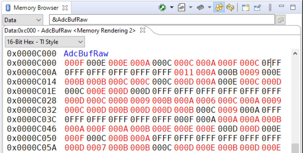
Next, we will check the ping pong buffer. In the memory browser, search for the address
&AdcBufRaw. Enable Continuous Refresh and ensure that you are viewing the memory in 16-bit hexadecimal. Watch the memory browser update in real-time. If all is well, you should notice thatAdcBufRawoccupies 100 16-bit memory locations and roughly 25% percent of the locations have a value of0x0FFFwhile the others contain something close to0x0000. This suggests that the DMA is transferring the ADC samples correctly into the ping pong buffer and the DMA ISR is correctly alternating the DMA channel 1 destination address pointer between the ping and pong buffers at the start of a transfer.
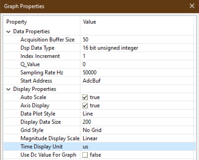
Now we will view the sampled PWM waveform in real-time using
AdcBuf. Click on Tools → Graph → Single TimeAcquisition Buffer Size: 50
Dsp Data Type: 16 bit unsigned integer
Sampling Rate Hz: 50000
Start Address: AdcBuf
Time Display Unit: us
Leave the other settings as their default value. Click OK and you should see the plot window open up.
Important
Note: If you do not see CCS menu Tools → Graph, please refer to Getting Started (Setting CCS for graph) to see the instruction on how to enable CCS graphing tool in your perspective.
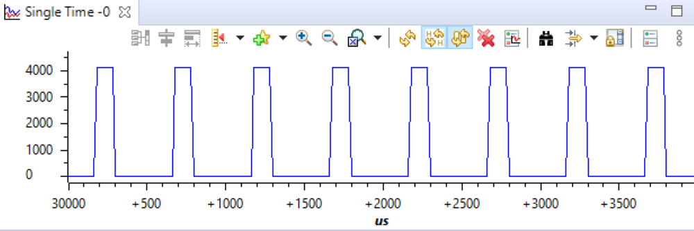
Activate the Continuous Refresh option in the plot window. You should now see several periods of the PWM waveform in the plot updating in real-time. If desired, you can use the measurement tool to verify that the duty cycle is 25% and the period is 500us. Leave the plot window open.
Finally, we will experiment with different values of delay in the DMA ISR. Add
OverCnt,TimDiff, andTaskDelayUsto the watch expression list and enable Continuous Refresh. Play with different values ofTaskDelayUsfrom 0–1000. Observe the changes inOverCntandTimDiff. At some point, you will find a value closer to 1000 that will causeOverCntto start to increment, which implies that the DMA is overwriting the contents of the next buffer. Even though the DMA is overwriting the next buffer, notice that the plot window appears to be unaffected. This is because the waveform we are viewing is periodic, thus, subsequent buffers will all contain the same information. However, if we were viewing an aperiodic waveform, we would be able to observe discontinuities and other artifacts in the signal due to the DMA overwriting the next buffer.Terminate the debug session and close the project. This concludes the lab assignment.
Full Solution#
The full solution to this lab exercise is included as part of the C2000Ware
SDK. Import the project from
[C2000Ware_Install_Path]/training/device/[device_name]/advance_topics/lab_dma.
Feedback
Please provide any feedback you may have about the content within this Academy to: c2000_academy_feedback@list.ti.com