Flash Introduction Lab#
Introduction#
This lab briefly introduces how to use the MSPM0 non-volatile memory (NVM) system for processing code and data. The tasks in this academy are based on examples from the MSPM0 SDK driver library, and demonstrate the following:
Writing values of different size to flash memory.
Reading and verifying values of different size from flash memory, and demonstrating a read verification error.
Writing 64-bit data to the flash memory and testing both single-bit error correction and double-bit error detection using ECC (Error Correction Code).
In total, there are 7 code examples relating to flash memory provided in the MSPM0 SDK. In this academy you will work with just the 3 examples discussed above to begin familiarizing yourself with the flash memory of MSPM0, while another 4 examples are available in case you want to further explore Flash memory use. The additional 4 SDK examples cover the following:
flashctl_program_with_ecc: Program a single flash word (64-bit data) with 8-bit ECC in MAIN memory.flashctl_blank_verify: Check whether the specified flash word at MAIN_BASE_ADDRESS is blank.flashctl_dynamic_memory_protection: Dynamically protect all of MAIN memory or a specific sector in MAIN memory.flashctl_nonmain_memory_write: Describe the user configuration structure and bootstrap loader configuration structure of the NONMAIN memory.
Note
This academy was originally written for the LP-MSPM0G3507 but it will also work with the LP-MSPM0L1306 LaunchPad. There may be small differences in the MSPM0L1306 examples, such as pinouts and launchpad connections, but overall you should still be able to easily complete the included tasks.
Prerequisites#
Hardware#
The following hardware is required for this lab:
Software#
The following software is required for this lab:
Installing the software#
Note
The software examples used for this lab should be imported from the TI Resource Explorer. This can be accessed from the web or locally in CCS by clicking View->Resource Explorer. Prior to importing a project, you first need to download the SDK in order to be able to import the examples to the CCS IDE. This may be done when CCS is installed or can be done later by clicking the “Download and Install” icon in the top right.
Recommended Resources#
These materials give a basic introduction to the MSPM0G MCU architecture and peripherals, which may help you understand the code examples and register configuration of the flash memory. If you have additional questions, please visit the TI E2E™ support forums to get help directly from our TI Experts.
Overview#
In order to understand flash memory and the code examples, it’s important to understand the basics of the MSPM0 flash system architecture. Within the MSPM0, flash memory is used for storing application code, data, the device boot configuration, and other critical parameters as defined by TI. Flash memory is typically divided into blocks based on volume, and throughout the code examples you will see the following terms used to refer to different pieces of flash memory depending on the size:
Term |
Definition |
Size |
|---|---|---|
Flash word |
Basic data size for programming and reading operations in the flash memory |
64 data bits (72 bits with ECC) |
Word line |
Group of flash words within a sector |
16 flash words |
Sector |
Group of word lines which are erased together (minimum erase resolution of flash memory) |
8 word lines |
Bank |
Group of sectors which can be mass erased in one operation |
Variable |
Region |
Logical assignment of a region of flash memory |
Variable |
Notice that these segments of flash memory are not just different in terms of size, but also in what operations can be performed on them. For example, the term Sector refers to the smallest amount of flash memory we can erase at once. Keeping in mind the flash memory divisions based on volume described above, the flash memory in the MSPM0G can also be divided into three regions based on intended use: FACTORY, NONMAIN, and MAIN. The FACTORY region is configured by TI for the device ID and other essential parameters. The NONMAIN region is usually for the device boot configuration, and the MAIN region is reserved for users, and is where your application code will typically be located. This table provides a basic summary of the different flash regions in MSPM0:
Term |
Region Contents |
Executable |
Used by |
Programmed by |
|---|---|---|---|---|
FACTORY |
Device ID and other parameters |
No |
Application |
TI only (not modifiable) |
NONMAIN |
Device boot configuration |
No |
Boot ROM |
TI / User |
MAIN |
Application code and data |
Yes |
Application |
User |
With the launchpad and code examples, this lab will walk you through using the MSPM0G flash memory step by step. You will see how to write and read different size values in flash and how to read back and and verify your operations were successful. As you work through the examples, pay attention to the memory browser window in CCS, to see how the flash memory updates as the code runs.
Getting Started#
Hardware Setup:#
To configure the MSPM0 LaunchPad for the SDK flash memory examples, you will simply need to connect the included USB cable to the launchpad to supply power, and enable programming, erasing and verification. Ensure as well that that the headers/jumpers are populated as shown in the image below.
Launchpad Input and Output diagram:#
ADC Connection#
Task 1 – Writing Data to Flash Memory#
1.1 Example Project Overview#
This task shows how to write multiple different sizes of data to the MAIN flash memory. In the example code, 8-bit, 16-bit, 32-bit, and 64-bit data are each written in sequence. The purpose is to display how to perform an erase of the flash memory in your program, and write data of different sizes.
To begin, let’s first program the MSPM0G3507 launchpad with the flashctl_multiple_size_write example to see how write operations are performed.
Import the flashctl_multiple_size_write example, flashctl_multiple_size_write into CCS from TI Resource Explorer. -MSPM0 SDK → Examples → Development Tools → LP-MSPM0G3507 Launchpad → DriverLib →
flashctl_multiple_size_writeClick import in the upper right hand corner
Build the code, and program it to the launchpad
1.2 Code Overview#
The basic structure of this code example can be broken down into:
Variable definition and system configuration
Erasing and writing to MAIN memory
LED control and main loop
1.2.1 Variable definition and system configuration:#
In this task, the application code and data are both written to the MAIN region of memory.
Before the operation, our example code defines the address in the MAIN region of memory that we wish to write to, and multiple different data variables of varying size. Here the MAIN address we want to write to is defined as
MAIN_BASE_ADDRESS (0x00001000). Because we know the size of this program once compiled, we have deliberately selected part of MAIN memory past the region that we need for our program. The variablesdata8,data16,data32,dataArray64[]are the 8-bit, 16-bit, 32-bit, and 64-bit data written to the flash memory, respectively. ThedataArray32[]is an array of 32-bit data to be written to the flash.
      #define MAIN_BASE_ADDRESS (0x00001000)

      uint8_t data8 = 0x11;
      uint16_t data16 = 0x2222;
      uint32_t data32 = 0x33333333;
      uint32_t dataArray64[] = {0xABCDEF00, 0x12345678};
      uint32_t dataArray32[] = {0x00000000, 0x11111111, 0x22222222, 0x33333333,
        0x4444, 0x55555, 0x66, 0x77, 0x8, 0x9}
In this code example, the power system and GPIO are configured at the very beginning of code execution. The configuration code can be found in
ti_msp_dl_config.c. The power supply of GPIO is initialized inSYSCFG_DL_initPower(void). The GPIO for the LED is initially configured inSYSCFG_DL_GPIO_init(void). The clock settings are applied inSYSCFG_DL_SYSCTL_init(void), the default MCU clock for this example is MCLK=SYSOSC=32 MHz, and LFCLK=LFOSC=32 kHz.
Note
Because this is example is a SysConfig enabled project, you will need to first build the code in order to generate the ti_msp_dl_config.c file. After building, this configuration file and the associated header file will appear in the project explorer in CCS, under the Generated Source header within your project folder.
      SYSCONFIG_WEAK void SYSCFG_DL_init(void)
      {
          SYSCFG_DL_initPower();
          SYSCFG_DL_GPIO_init();
          /* Module-Specific Initializations*/
          SYSCFG_DL_SYSCTL_init();
      }

      void SYSCFG_DL_initPower(void)
      {
          DL_GPIO_reset(GPIOA);
          DL_GPIO_reset(GPIOB);

          DL_GPIO_enablePower(GPIOA);
          DL_GPIO_enablePower(GPIOB);
          delay_cycles(POWER_STARTUP_DELAY);
      }

      void SYSCFG_DL_GPIO_init(void)
      {
          DL_GPIO_initDigitalOutput(GPIO_LEDS_USER_LED_1_IOMUX);

          DL_GPIO_enableOutput(GPIO_LEDS_PORT, GPIO_LEDS_USER_LED_1_PIN);
          DL_GPIO_clearPins(GPIO_LEDS_PORT, GPIO_LEDS_USER_LED_1_PIN);
      }

      SYSCONFIG_WEAK void SYSCFG_DL_SYSCTL_init(void)
      {
          DL_SYSCTL_setSYSOSCFreq(DL_SYSCTL_SYSOSC_FREQ_BASE);
          DL_SYSCTL_setMCLKDivider(DL_SYSCTL_MCLK_DIVIDER_DISABLE);
          DL_SYSCTL_setULPCLKDivider(DL_SYSCTL_ULPCLK_DIV_1);

          //Low Power Mode is configured to be SLEEP0
          DL_SYSCTL_setBORThreshold(DL_SYSCTL_BOR_THRESHOLD_LEVEL_0);
      }
1.2.2 Erasing and writing to MAIN memory:#
In this portion of the flash write code example, within the main function we do the following:
Unprotect and erase the specified sector in the MAIN memory.
        DL_FlashCTL_unprotectSector(
            FLASHCTL, MAIN_BASE_ADDRESS, DL_FLASHCTL_REGION_SELECT_MAIN);
        DL_FlashCTL_eraseMemory(
            FLASHCTL, MAIN_BASE_ADDRESS, DL_FLASHCTL_COMMAND_SIZE_SECTOR);
Write 8-bit, 16-bit, 32-bit and 64-bit data to the MAIN memory, using ECC. Versions of these driverlib functions without ECC generated also exist. Because the target program address must be a flash word address (8-byte aligned), we increase the address we are writing in increments of 8, even if we aren’t using the whole flash word. At the end of each program command we wait for the completion of the write using a call to
DL_FlashCTL_waitForCmdDone.
        DL_FlashCTL_unprotectSector(
            FLASHCTL, MAIN_BASE_ADDRESS, DL_FLASHCTL_REGION_SELECT_MAIN);
        DL_FlashCTL_programMemory8WithECCGenerated(
            FLASHCTL, MAIN_BASE_ADDRESS, &data8);
        DL_FlashCTL_waitForCmdDone(FLASHCTL);

        DL_FlashCTL_unprotectSector(
            FLASHCTL, MAIN_BASE_ADDRESS, DL_FLASHCTL_REGION_SELECT_MAIN);
        DL_FlashCTL_programMemory16WithECCGenerated(
            FLASHCTL, (MAIN_BASE_ADDRESS + 8), &data16);
        DL_FlashCTL_waitForCmdDone(FLASHCTL);

        DL_FlashCTL_unprotectSector(
            FLASHCTL, MAIN_BASE_ADDRESS, DL_FLASHCTL_REGION_SELECT_MAIN);
        DL_FlashCTL_programMemory32WithECCGenerated(
            FLASHCTL, (MAIN_BASE_ADDRESS + 16), &data32);
        DL_FlashCTL_waitForCmdDone(FLASHCTL);

        DL_FlashCTL_unprotectSector(
            FLASHCTL, MAIN_BASE_ADDRESS, DL_FLASHCTL_REGION_SELECT_MAIN);
        DL_FlashCTL_programMemory64WithECCGenerated(
            FLASHCTL, (MAIN_BASE_ADDRESS + 24), &dataArray64[0]);
        DL_FlashCTL_waitForCmdDone(FLASHCTL);
1.2.3 LED control and main loop:#
At the end of this code example, the LED status is set to indicate the programming has completed.
After programming, a software breakpoint is set, so that we can check the contents of the MCU flash memory in the memory browser of CCS. Inside the while loop after the software breakpoint, the call the __WFI() causes the MSPM0 to enter the configured low power mode.
     DL_GPIO_setPins(GPIO_LEDS_PORT, GPIO_LEDS_USER_LED_1_PIN);
     __BKPT(0);

     while (1) {
         __WFI();
     }
1.3 Code Execution#
Connect the PC to the LaunchPad using the Micro USB cable. In CCS, build the example code and launch a debug session. Click View→Memory Browser and open the Memory Browser.
After the launchpad is programmed, input the MAIN_BASE_ADDRESS (0x00001000) into the memory browser, and click on the resume button in the menu bar to execute the code. The memory browser shows the updated values marked in red, and should be consistent with what we have written to the flash memory. As shown in the image, the first 8-bit data is written aligned with MAIN_BASE_ADDRESS. Then, the second 16-bit data is written aligned with MAIN_BASE_ADDRESS+8 and the third data is written aligned with MAIN_BASE_ADDRESS+16. The fourth data is written aligned with MAIN_BASE_ADDRESS+24. All of this data is stored in Little-endian format. In addition to the updated memory values, you should see LED1 turn on when the write operations are complete.
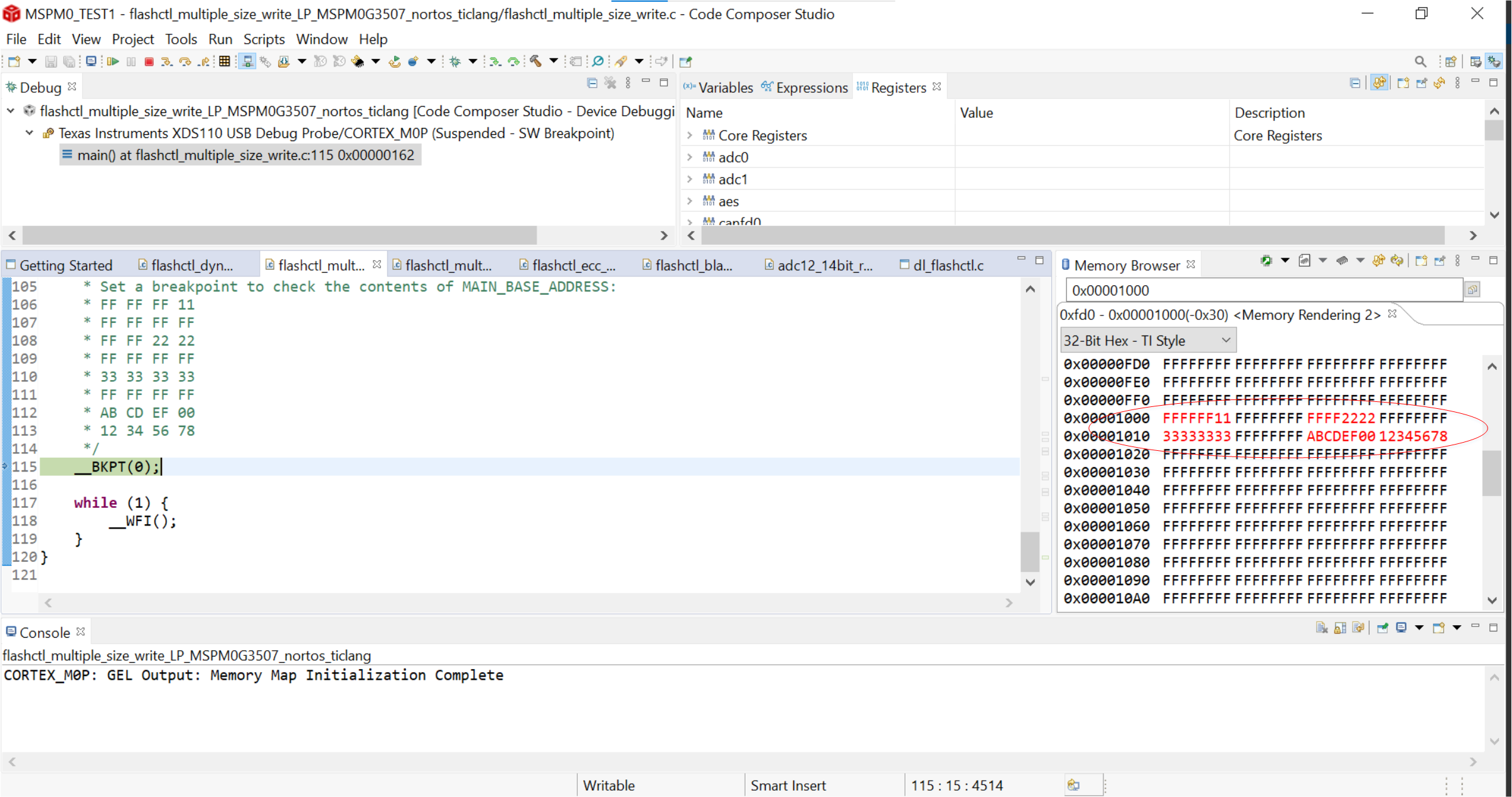
Flash Write Data#
Now that you are familiar with how this example works, try modifying the code so that the data is stored elsewhere in MAIN memory, and watching the memory browser window to verify this is happening as you expect. One potential solution is given below.
Solution to storing data elsewhere in flash memory
Recall that MAIN_BASE_ADDRESS (0x00001000) is defined at the beginning of the example code as the base memory address for where we want to write in flash. Let’s try updating the value of MAIN_BASE_ADDRESS from 0x1000, to 0x2000.
/* Address in main memory to write to */
#define MAIN_BASE_ADDRESS (0x00002000)
With the LaunchPad connected to your PC via the usb cable, we can then launch a debug session to build and program the device as we did before. In the memory browser window, enter the address 0x2000, and press enter. Then hit the resume button in the CCS toolbar to begin executing the code from main. After you hit the breakpoint at the end of the code, you should see the updated red text values as before, but now at address 0x2000.
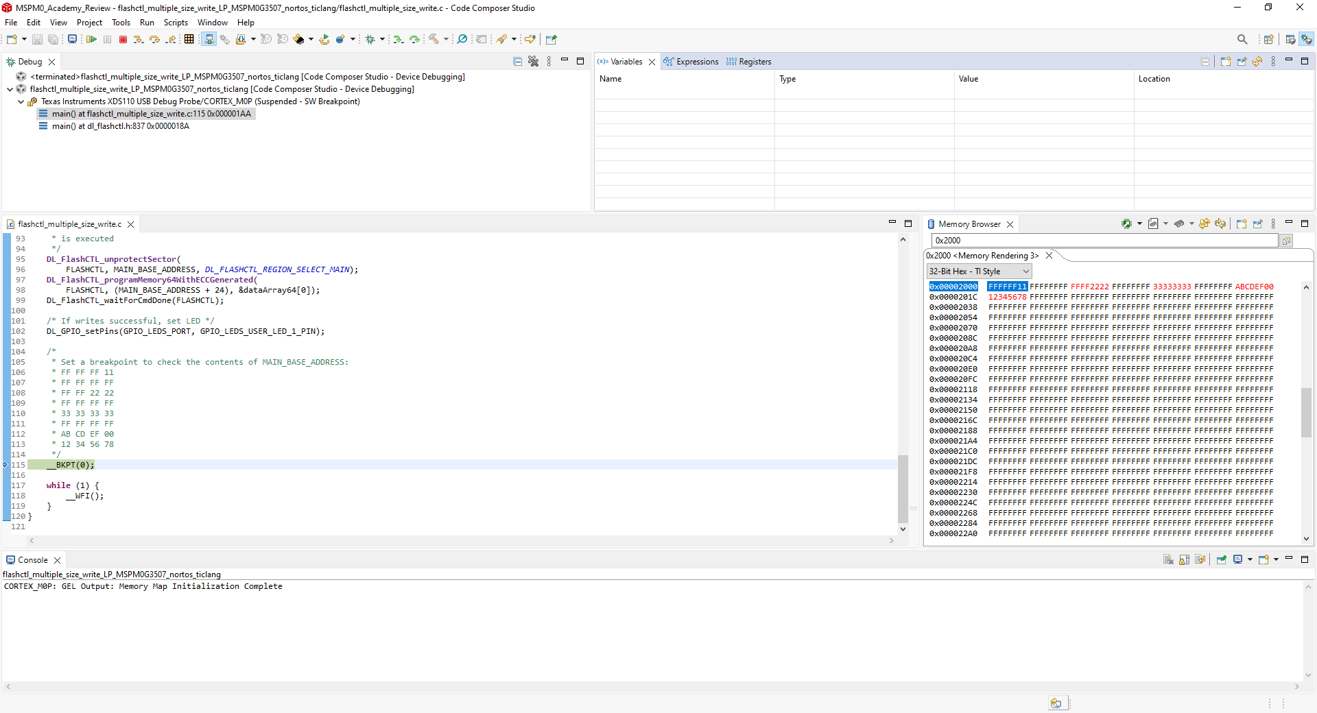
Flash Write Data now at 0x2000#
What is the last address in flash memory for the MSPM0G3507, and what do you see in the memory browser in CCS if you try to look beyond this? (Hint: Look at the MSPM0G3507 datasheet, at the Detailed Description→Memory section to find the end address of MAIN memory)
Task 2 – Reading Data from Flash Memory#
2.1 Example Project Overview#
This task shows how to read back and verify data of multiple different sizes that has been written in the MAIN region of flash memory. In this example, an incorrect piece of 64-bit data is also written to demonstrate verification upon a failed read. This shows how to read back written data from Flash memory and verify if an error or data corruption has occurred.
To begin, let’s program the MSPM0G3507 launchpad with the flashctl_multiple_size_read_verify example.
Import the flashctl_multiple_size_read_verify example flashctl_multiple_size_read_verify into CCS from TI Resource Explorer. -MSPM0 SDK → Examples → Development Tools → LP-MSPM0G3507 Launchpad → DriverLib →
flashctl_multiple_size_read_verifyClick import in the upper right hand corner
Build the code and program the launchpad by launching a debug session in CCS.
2.2 Code Overview#
Similar to Task 1, the basic structure of this code example can be divided into 3 parts:
Variable definition and system configuration
Writing, reading, and verifying data in MAIN memory
Main loop
2.2.1 Variable definition and system configuration:#
In this example, the application code and data are written to the MAIN region of the flash.
Before the operation, the MAIN region address and data variables of multiple sizes are predefined. Notice that the error data and error ECC code values are also defined here. The main address is defined the same as previously, as MAIN_BASE_ADDRESS (0x00001000). The 8-bit, 16-bit, 32-bit and 64-bit data are defined as
gData8,gData16,gData32andgDataArray64[], respectively. The variablegDataArray64Error[]is used as the bad data to test read back verification. Next, the EEC value is defined for the 64-bit data in the MAIN memory manually. And the error ECC code is defined to demonstrate a failed read verification.
   #define MAIN_BASE_ADDRESS (0x00001000)
   uint8_t gData8 = 0x11;
   uint16_t gData16 = 0x2222;
   uint32_t gData32 = 0x33333333;
   uint32_t gDataArray64[] = {0xABCDEF00, 0x12345678};
   uint32_t gDataArray64Error[] = {0x00FEDCBA, 0x87654321};
   uint8_t gECCCode = 0xAF;
   uint8_t gECCCodeError = 0xBC;
In this code example, the configuration of the power mode, GPIO, and SYSCTL are the same as in Task 1.
2.2.2 Writing, reading, and verifying data in MAIN memory#
In this code example, the main function consists of the following:
Unprotect and erase the specified sector in the MAIN memory.
   /* Erase sector in main memory */
   DL_FlashCTL_unprotectSector(
       FLASHCTL, MAIN_BASE_ADDRESS, DL_FLASHCTL_REGION_SELECT_MAIN);
   DL_FlashCTL_eraseMemory(
       FLASHCTL, MAIN_BASE_ADDRESS, DL_FLASHCTL_COMMAND_SIZE_SECTOR);
   DL_FlashCTL_waitForCmdDone(FLASHCTL);
Write 8-bit, 16-bit, 32-bit and 64-bit data to the MAIN memory, with the corresponding reading actions performed after. Before each write/read operation, the MAIN sector is unprotected and the data is written to the flash memory. Then, the data is read and verified with a software breakpoint set to help you observe the variables as they change.
   /* 8-bit write to flash in main memory */
   DL_FlashCTL_unprotectSector(
       FLASHCTL, MAIN_BASE_ADDRESS, DL_FLASHCTL_REGION_SELECT_MAIN);
   DL_FlashCTL_programMemory8(FLASHCTL, MAIN_BASE_ADDRESS, &gData8);
   DL_FlashCTL_waitForCmdDone(FLASHCTL);

   /* Read verify on the 8-bit data */
   DL_FlashCTL_readVerify8(FLASHCTL, MAIN_BASE_ADDRESS, &gData8);
   DL_FlashCTL_waitForCmdDone(FLASHCTL);
   /* Set a breakpoint if read verify fails */
   failType = DL_FlashCTL_getFailureStatus(FLASHCTL);
   if (failType != DL_FLASHCTL_FAIL_TYPE_NO_FAILURE) {
       __BKPT(0);
   }

   /* 16-bit write to flash in main memory  */
   DL_FlashCTL_unprotectSector(
       FLASHCTL, MAIN_BASE_ADDRESS, DL_FLASHCTL_REGION_SELECT_MAIN);
   DL_FlashCTL_programMemory16(FLASHCTL, (MAIN_BASE_ADDRESS + 8), &gData16);
   DL_FlashCTL_waitForCmdDone(FLASHCTL);

   /* Read verify on the 16-bit data */
   DL_FlashCTL_readVerify16(FLASHCTL, (MAIN_BASE_ADDRESS + 8), &gData16);
   DL_FlashCTL_waitForCmdDone(FLASHCTL);
   /* Set a breakpoint if read verify fails */
   failType = DL_FlashCTL_getFailureStatus(FLASHCTL);
   if (failType != DL_FLASHCTL_FAIL_TYPE_NO_FAILURE) {
       __BKPT(0);
   }

   /* 32-bit write to flash in main memory */
   DL_FlashCTL_unprotectSector(
       FLASHCTL, MAIN_BASE_ADDRESS, DL_FLASHCTL_REGION_SELECT_MAIN);
   DL_FlashCTL_programMemory32(FLASHCTL, (MAIN_BASE_ADDRESS + 16), &gData32);
   DL_FlashCTL_waitForCmdDone(FLASHCTL);

   /* Read verify on the 32-bit data */
   DL_FlashCTL_readVerify32(FLASHCTL, (MAIN_BASE_ADDRESS + 16), &gData32);
   DL_FlashCTL_waitForCmdDone(FLASHCTL);
   /* Set a breakpoint if read verify fails */
   failType = DL_FlashCTL_getFailureStatus(FLASHCTL);
   if (failType != DL_FLASHCTL_FAIL_TYPE_NO_FAILURE) {
       __BKPT(0);
   }

   /* 64-bit write to flash in main memory */
   DL_FlashCTL_unprotectSector(
       FLASHCTL, MAIN_BASE_ADDRESS, DL_FLASHCTL_REGION_SELECT_MAIN);
   DL_FlashCTL_programMemory64(
       FLASHCTL, (MAIN_BASE_ADDRESS + 24), &gDataArray64[0]);
   DL_FlashCTL_waitForCmdDone(FLASHCTL);

   /* Read verify on the 64-bit data */
   DL_FlashCTL_readVerify64(
       FLASHCTL, (MAIN_BASE_ADDRESS + 24), &gDataArray64[0]);
   DL_FlashCTL_waitForCmdDone(FLASHCTL);
   /* Set a breakpoint if read verify fails */
   failType = DL_FlashCTL_getFailureStatus(FLASHCTL);
   if (failType != DL_FLASHCTL_FAIL_TYPE_NO_FAILURE) {
       __BKPT(0);
   }

   /* Demonstrate a failed read verify when data does not match */
   DL_FlashCTL_readVerify64(
       FLASHCTL, (MAIN_BASE_ADDRESS + 24), &gDataArray64Error[0]);
   DL_FlashCTL_waitForCmdDone(FLASHCTL);
   /* Set a breakpoint if read verify does not fail */
   failType = DL_FlashCTL_getFailureStatus(FLASHCTL);
   if (failType != DL_FLASHCTL_FAIL_TYPE_VERIFY_ERROR) {
       __BKPT(0);
   }

   /*
    * 64-bit write to flash in main memory, with ECC enabled and generated
    * by flash controller hardware
    */
   DL_FlashCTL_unprotectSector(
       FLASHCTL, MAIN_BASE_ADDRESS, DL_FLASHCTL_REGION_SELECT_MAIN);
   DL_FlashCTL_programMemory64WithECCGenerated(
       FLASHCTL, (MAIN_BASE_ADDRESS + 32), &gDataArray64[0]);
   DL_FlashCTL_waitForCmdDone(FLASHCTL);

   /*
    * Read verify on the 64-bit data, with ECC enabled and generated
    * by flash controller hardware
    */
   DL_FlashCTL_readVerify64WithECCGenerated(
       FLASHCTL, (MAIN_BASE_ADDRESS + 32), &gDataArray64[0]);
   DL_FlashCTL_waitForCmdDone(FLASHCTL);
   /* Set a breakpoint if read verify fails */
   failType = DL_FlashCTL_getFailureStatus(FLASHCTL);
   if (failType != DL_FLASHCTL_FAIL_TYPE_NO_FAILURE) {
       __BKPT(0);
   }
Bad data verification and an incorrect ECC value are then used to demonstrate the effectiveness of read verification. First, the
gDataArray64Error[]is used as the written data to cause a reading error. A software breakpoint is also set here to allow observation of the reading status when running in debug mode. Then, thegDataArray64[]is written in the specified memory with thegECCCodemanually. Next, thegDataArray64Error[]andgECCCodeErrorare used to demonstrate a reading error combined with EEC. More software breakpoints are inserted as needed.
   /* Demonstrate a failed read verify when data does not match */
   DL_FlashCTL_readVerify64(
       FLASHCTL, (MAIN_BASE_ADDRESS + 24), &gDataArray64Error[0]);
   DL_FlashCTL_waitForCmdDone(FLASHCTL);
   /* Set a breakpoint if read verify does not fail */
   failType = DL_FlashCTL_getFailureStatus(FLASHCTL);
   if (failType != DL_FLASHCTL_FAIL_TYPE_VERIFY_ERROR) {
       __BKPT(0);
   }

   /*
    * 64-bit write to flash in main memory, with ECC enabled and generated
    * by flash controller hardware
    */
   DL_FlashCTL_unprotectSector(
       FLASHCTL, MAIN_BASE_ADDRESS, DL_FLASHCTL_REGION_SELECT_MAIN);
   DL_FlashCTL_programMemory64WithECCGenerated(
       FLASHCTL, (MAIN_BASE_ADDRESS + 32), &gDataArray64[0]);
   DL_FlashCTL_waitForCmdDone(FLASHCTL);

   /*
    * Read verify on the 64-bit data, with ECC enabled and generated
    * by flash controller hardware
    */
   DL_FlashCTL_readVerify64WithECCGenerated(
       FLASHCTL, (MAIN_BASE_ADDRESS + 32), &gDataArray64[0]);
   DL_FlashCTL_waitForCmdDone(FLASHCTL);
   /* Set a breakpoint if read verify fails */
   failType = DL_FlashCTL_getFailureStatus(FLASHCTL);
   if (failType != DL_FLASHCTL_FAIL_TYPE_NO_FAILURE) {
       __BKPT(0);
   }

   /*
    * 64-bit write to flash in main memory, with manually provided ECC code
    * after overriding ECC generated by the flash controller hardware
    */
   DL_FlashCTL_enableOverrideHardwareGeneratedECC(FLASHCTL);
   DL_FlashCTL_unprotectSector(
       FLASHCTL, MAIN_BASE_ADDRESS, DL_FLASHCTL_REGION_SELECT_MAIN);
   DL_FlashCTL_programMemory64WithECCManual(
       FLASHCTL, (MAIN_BASE_ADDRESS + 40), &gDataArray64[0], &gECCCode);
   DL_FlashCTL_waitForCmdDone(FLASHCTL);

   /*
    * Read verify on the 64-bit data, with ECC enabled and generated
    * by flash controller hardware
    */
   DL_FlashCTL_readVerify64WithECCManual(
       FLASHCTL, (MAIN_BASE_ADDRESS + 40), &gDataArray64[0], &gECCCode);
   DL_FlashCTL_waitForCmdDone(FLASHCTL);
   /* Set a breakpoint if read verify fails */
   failType = DL_FlashCTL_getFailureStatus(FLASHCTL);
   if (failType != DL_FLASHCTL_FAIL_TYPE_NO_FAILURE) {
       __BKPT(0);
   }

   /* Demonstrate a failed read verify when ECC code does not match */
   DL_FlashCTL_readVerify64WithECCManual(FLASHCTL, (MAIN_BASE_ADDRESS + 40),
       &gDataArray64Error[0], &gECCCodeError);
   DL_FlashCTL_waitForCmdDone(FLASHCTL);
   /* Set a breakpoint if read verify does not fail */
   failType = DL_FlashCTL_getFailureStatus(FLASHCTL);
   if (failType != DL_FLASHCTL_FAIL_TYPE_VERIFY_ERROR) {
       __BKPT(0);
   }

   DL_FlashCTL_disableOverrideHardwareGeneratedECC(FLASHCTL);
2.2.3 Main loop#
In this example, once the end of main is reached, the LED is toggled the LED status is toggled inside the main while loop.
/* After completion, toggle LED */
while (1) {
    DL_GPIO_togglePins(GPIO_LEDS_PORT, GPIO_LEDS_USER_LED_1_PIN);
    delay_cycles(16000000);
}
2.3 Code Execution#
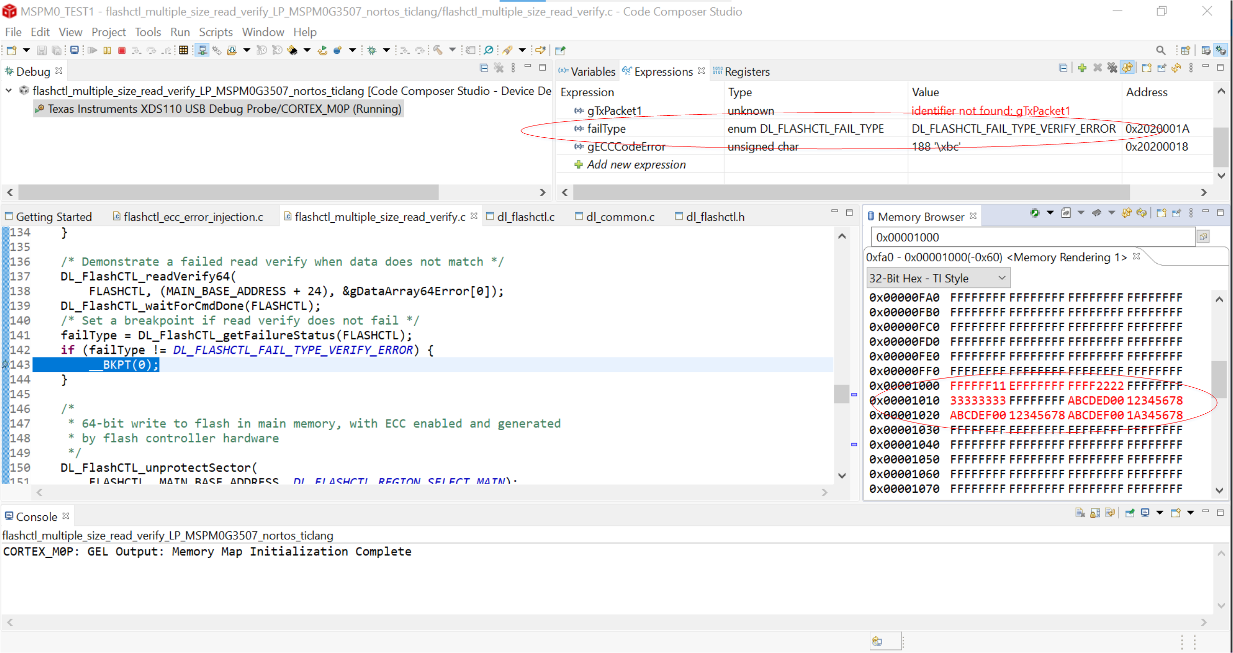
Connect the PC to the LaunchPad using the included micro USB cable. In CCS, build the example code and program the launchpad by launching a debug session. Click View→Memory Browser and open the Memory Browser. Within the code editor, highlight the variable failType, right click it and in the context menu select Add Watch Expression, while debugging, you will be able to view the value of this variable in the expressions window. While debugging, the variable failType, will indicate the status of a read when the read action occurs.
After the launchpad finishes programming and the debugger is connected, the code will be at main and ready to execute. In the Memory Browser window, input the MAIN_BASE_ADDRESS (0x00001000). The values in red indicate updates to the flash memory since the last breakpoint, and will stay consistent with what we have written to flash memory. When the 8 bit, 16-bit, 32-bit, and 64 bit correct data is written and verified, the variable failType is kept as DL_FLASHCTL_FAIL_TYPE_NO_FAILURE, which indicates that a reading error has not occurred. When the 64-bit incorrect data or incorrect ECC value is used for reading verification, the variable failType is set as DL_FLASHCTL_FAIL_TYPE_VERIFY_ERROR, which indicates that a reading error has occurred. From the memory browser, you can check the data written to the flash memory based on the specified address.
Note that you can also open the register window by selecting View→Registers, in order to view the values of the CMDDATA0 and CMDDATA1 registers. These registers are used for flash write and read operations. The data to be verified is written to the above registers before reading verification.
The LED status is toggled inside the main loop if the previous operations are executed as expected and no breakpoint is triggered. No breakpoint will be trigged by the invalid operations with the example code as written, but you can either set a breakpoint at the checks for the value of failType, or change the conditionals to deliberately cause a software breakpoint to be hit. This will allow you to view the value of failType at specific points in the program.
Flash Read Data#
Task 3 – ECC Error Injection in Flash Memory#
3.1 Example Project Overview#
When used alongside memory, an error correction code, or ECC, helps maintain the integrity of data stored in flash memory by correcting or detecting data corruption. Every 8 bit error correction code in MSPM0G is associated with a corresponding 64 bit flash word. This task briefly describes that how the ECC module works in MSPM0G when single-bit and double-bit data errors occur. In this example, the ECC code is first generated according to the correct 64-bit data. Then, a single-bit and double-bit error with the ECC code are deliberately tested to demonstrate ECC verification and protection.
To begin, Let’s program the MSPM0G3507 launchpad with the flashctl_ecc_error_injection example.
Import the flashctl_ecc_error_injection example flashctl_ecc_error_injection into CCS from TI Resource Explorer. -MSPM0 SDK → Examples → Development Tools → LP-MSPM0G3507 Launchpad → DriverLib →
flashctl_ecc_error_injectionClick import in the upper right hand corner
Build the code and program the launchpad by launching a debug session in CCS.
3.2 Code Overview#
Similar to the previous tasks, the basic structure of this code example can be divided into 3 parts:
Variable definition and system configuration
ECC error detection and correction
Main loop
3.2.1 Variable definition and system configuration:#
In this example, both the application code and sample data are written to the MAIN region of the flash.
Before the operation, the MAIN region address is defined as MAIN_BASE_ADDRESS (0x00001000). The ECC code address is defined as ECC_CODE_ADDRESS_SPACE (0x41801000). The corrected and the uncorrected data address are defined as CORRECTED_ADDRESS_SPACE (0x00001000) and UNCORRECTED_ADDRESS_SPACE (0x00401000), respectively. Notice that the 64-bit correct data
gDataArray64[]and the corresponding single-bit error datagDataArray64SEC[]are different from the correct data only by the least significant bit. Similarly, the value ingDataArray64DED[]is the correct data with the 2 least significant bits both modified.
     #define MAIN_BASE_ADDRESS (0x00001000)
     #define ECC_CODE_ADDRESS_SPACE (0x41801000)
     #define CORRECTED_ADDRESS_SPACE (0x00001000)
     #define UNCORRECTED_ADDRESS_SPACE (0x00401000)

     uint32_t gDataArray64[] = {0xABCDEF00, 0x12345678};
     uint32_t gDataArray64SEC[] = {0xABCDEF01, 0x12345678};
     uint32_t gDataArray64DED[] = {0xABCDEF11, 0x12345678};
In this example, the configuration of the power mode, GPIO, and SYSCTL are the same as in Task 1.
3.2.2 ECC error detection and correction:#
In this code example, the ECC code address, the uncorrected data address, and the corrected data address are all already defined as pre-processor directives. The variables uncorrectedData and correctedData are also defined as well as the error status and the ECC code. The initial 64-bit values are written to the MAIN memory and the ECC values are generated automatically.
   uint32_t* eccCodeAddress     = (void*) ECC_CODE_ADDRESS_SPACE;
   uint32_t* uncorrectedAddress = (void*) UNCORRECTED_ADDRESS_SPACE;
   uint32_t* correctedAddress   = (void*) CORRECTED_ADDRESS_SPACE;
   uint32_t uncorrectedData __attribute__((unused));
   uint32_t correctedData __attribute__((unused));
   uint32_t status __attribute__((unused));
   uint8_t eccCode;

   /* Erase memory before programming */
   DL_FlashCTL_unprotectSector(
       FLASHCTL, MAIN_BASE_ADDRESS, DL_FLASHCTL_REGION_SELECT_MAIN);
   DL_FlashCTL_eraseMemory(
       FLASHCTL, MAIN_BASE_ADDRESS, DL_FLASHCTL_COMMAND_SIZE_SECTOR);
   DL_FlashCTL_waitForCmdDone(FLASHCTL);

   /*
    * Program single flash word (64-bit data) with ECC enabled.
    * The flash controller hardware will handle generating the 8-bit ECC code.
    */
   DL_FlashCTL_unprotectSector(
       FLASHCTL, MAIN_BASE_ADDRESS, DL_FLASHCTL_REGION_SELECT_MAIN);
   DL_FlashCTL_programMemory64WithECCGenerated(
       FLASHCTL, (MAIN_BASE_ADDRESS), &gDataArray64[0]);
   DL_FlashCTL_waitForCmdDone(FLASHCTL);
   /* Get the 8-bit ECC code that was generated for this 64-bit data */
   eccCode = *(eccCodeAddress);

   /* Erase the sector */
   DL_FlashCTL_unprotectSector(
       FLASHCTL, MAIN_BASE_ADDRESS, DL_FLASHCTL_REGION_SELECT_MAIN);
   DL_FlashCTL_eraseMemory(
       FLASHCTL, MAIN_BASE_ADDRESS, DL_FLASHCTL_COMMAND_SIZE_SECTOR);
   DL_FlashCTL_waitForCmdDone(FLASHCTL);
Next, the single-bit error value is written to the flash memory using the non-erroneous ECC value. Then, a software breakpoint is set to allow us to observe the result of this operation in memory.
   /*
    * Enable override of hardware generated ECC. This allows the user to
    * manually set the ECC code to be programmed.
    */
   DL_FlashCTL_enableOverrideHardwareGeneratedECC(FLASHCTL);

   /*
    * Demonstrate a SEC (single bit error correction) error.
    * Program 64-bit data with ECC enabled, but the data in gDataArray64SEC
    * has a one bit difference from the data in gDataArray64.
    * Additionally, the ECC code being programmed corresponds with the data
    * in gDataArray64. Since we are using the ECC code corresponding with
    * gDataArray64, and gDataArray64SEC has a bit difference in the data,
    * this will trigger a SEC error.
    */
   DL_SYSCTL_clearECCErrorStatus();
   DL_FlashCTL_unprotectSector(
       FLASHCTL, MAIN_BASE_ADDRESS, DL_FLASHCTL_REGION_SELECT_MAIN);
   DL_FlashCTL_programMemory64WithECCManual(
       FLASHCTL, (MAIN_BASE_ADDRESS), &gDataArray64SEC[0], &eccCode);
   DL_FlashCTL_waitForCmdDone(FLASHCTL);

   /*
    * The status variable will have value DL_SYSCTL_STATUS_FLASH_SEC.
    * The uncorrected address space has the original raw data of
    * gDataArray64SEC. The corrected address space has the ECC-corrected data.
    * Since there was only a single bit error, this is a correctable error, so
    * the 'corrected' data that matched the manually provided ECC code was
    * programmed. The 'corrected' data of gDataArray64SEC will match the data
    * of gDataArray64
    */
   uncorrectedData = *uncorrectedAddress;
   correctedData   = *correctedAddress;
   /* Delay in order for register to update status accordingly */
   delay_cycles(1000000);
   status = DL_SYSCTL_getStatus() & DL_SYSCTL_STATUS_FLASH_SEC;

   /*
    * Set a breakpoint to confirm the values of:
    * status = DL_SYSCTL_STATUS_FLASH_SEC
    * uncorrectedData = {0xABCDEF01, 0x12345678}
    * correctedData = {0xABCDEF00, 0x12345678}
    * User can also check the memory browser at addresses
    * CORRECTED_ADDRESS_SPACE and UNCORRECTED_ADDRESS_SPACE
    */
   __BKPT(0);

   /* Erase the sector */
   DL_FlashCTL_unprotectSector(
       FLASHCTL, MAIN_BASE_ADDRESS, DL_FLASHCTL_REGION_SELECT_MAIN);
   DL_FlashCTL_eraseMemory(
       FLASHCTL, MAIN_BASE_ADDRESS, DL_FLASHCTL_COMMAND_SIZE_SECTOR);
   DL_FlashCTL_waitForCmdDone(FLASHCTL);
Finally, the double-bit error value is written to the flash memory with the non-erroneous ECC value. Again, a breakpoint is set to allow us to observe the results.
   /*
    * Demonstrate a DED (double bit error correction) error.
    * Program 64-bit data with ECC enabled, but the data in gDataArray64DED
    * has a two bit difference from the data in gDataArray64.
    * Additionally, the ECC code being programmed corresponds with the data in
    * gDataArray64. Since we are using the ECC code corresponding with
    * gDataArray64, and gDataArray64DED has a two bit difference in the data,
    * this will trigger a DED error.
   */
   DL_SYSCTL_clearECCErrorStatus();
   DL_FlashCTL_unprotectSector(
       FLASHCTL, MAIN_BASE_ADDRESS, DL_FLASHCTL_REGION_SELECT_MAIN);
   DL_FlashCTL_programMemory64WithECCManual(
       FLASHCTL, (MAIN_BASE_ADDRESS), &gDataArray64DED[0], &eccCode);
   DL_FlashCTL_waitForCmdDone(FLASHCTL);

   /*
    * The status variable will have value DL_SYSCTL_STATUS_FLASH_DED.
    * The uncorrected address space has the original raw data of gDataArray64DED.
    * The corrected address space has the ECC-corrected data, but since there was
    * a double bit error and this type of error is uncorrectable, the data at
    * the corrected address space will also be the data of gDataArray64DED.
   */
   correctedData   = *correctedAddress;
   uncorrectedData = *uncorrectedAddress;
   /* Delay in order for register to update status accordingly */
   delay_cycles(1000000);
   status = DL_SYSCTL_getStatus() & DL_SYSCTL_STATUS_FLASH_DED;

   /*
    * Set a breakpoint to confirm the values of:
    * status = DL_SYSCTL_STATUS_FLASH_DED
    * uncorrectedData = {0xABCDEF11, 0x12345678}
    * correctedData = {0xABCDEF11, 0x12345678}
    * User can also check the memory browser at addresses
    * CORRECTED_ADDRESS_SPACE and UNCORRECTED_ADDRESS_SPACE
    */
   __BKPT(0);

   /* Disable override of hardware generated ECC. */
   DL_FlashCTL_disableOverrideHardwareGeneratedECC(FLASHCTL);
3.2.3 Main loop:#
In this code example, the main loop is identical to that in the task 2.
3.3 Code Execution#
Connect the LaunchPad to the PC using the micro USB cable. In CCS, build the example code and program the launchpad. Click View→Memory Browser and Open the Memory Browser. Highlight the variable status, right click on it and in the context menu select Add Watch Expression, you should then see this variable appear in the expressions window. After we hit the software breakpoints in the code, we will see this variable update to indicate the ECC Error type.
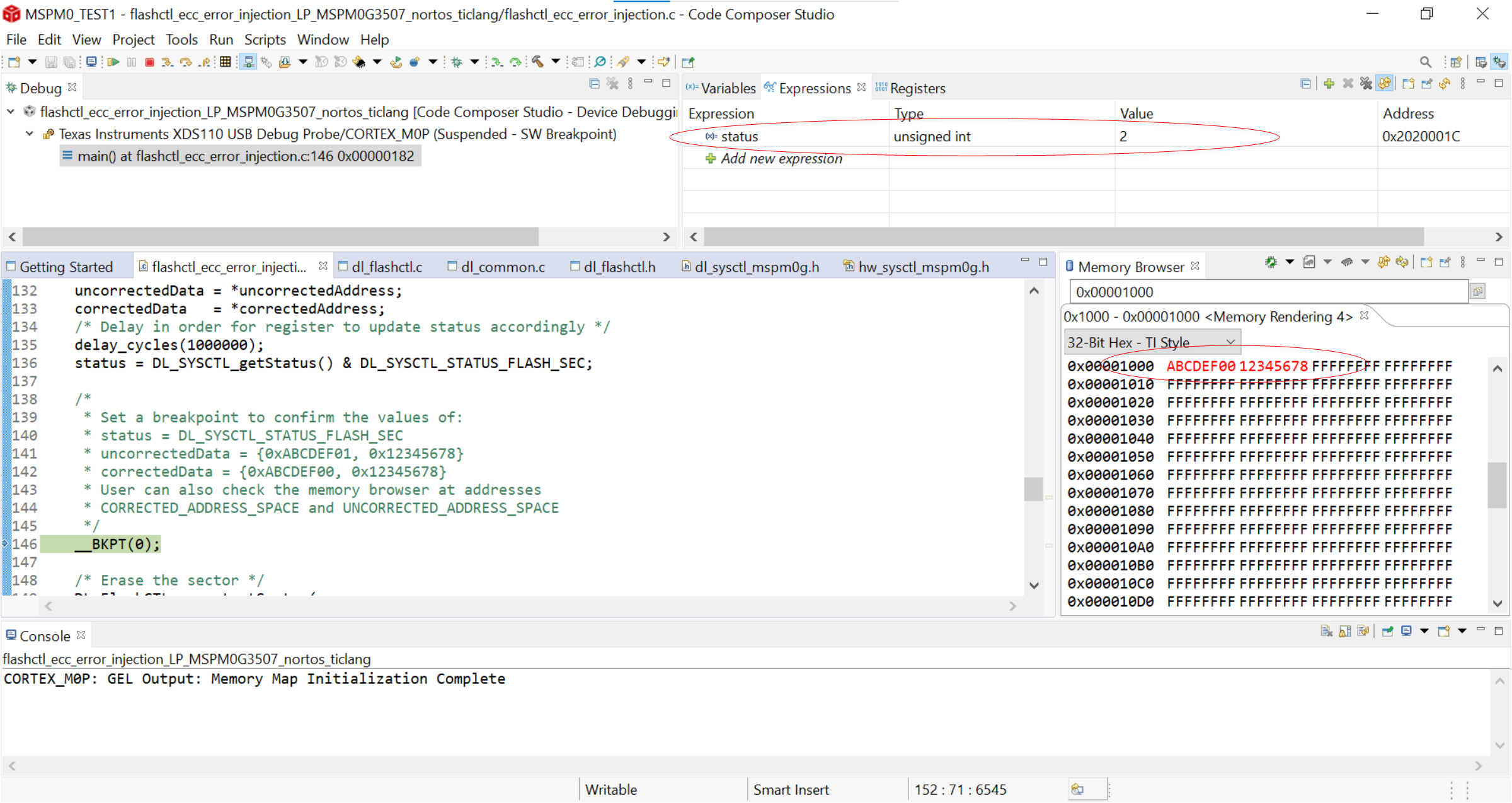
After the launchpad finishes programming and the debugger is connected, the code will be at main and ready to execute. In the Memory Browser window, input the MAIN_BASE_ADDRESS (0x00001000). The values in red indicate updates to the flash memory since the last breakpoint, and will reflect what we have written to flash memory. At the first breakpoint, the 64-bit data with single-bit error triggers a SEC (single error correction) error, and the variable status is set to 2. In flash memory, you should see that the error is corrected, and the “correct” value is what is actually loaded. The single-bit error data we tried to write is {0xABCDEF01, 0x12345678}, while the corrected data that is actually written is {0xABCDEF00, 0x12345678}, which is the same as the gDataArray64[]. This shows that the SEC error is correctable.
Note
The status variable may be optimized out depending on your compiler and project settings. To correct this with TIClang in CCS, right click on your project in the project browser, and select Properties from the context menu. In the Project Options dialog box which opens, navigate to Build→Arm Compiler→Optimization, and set your optimization level to the minimum.
Flash ECC Code1#
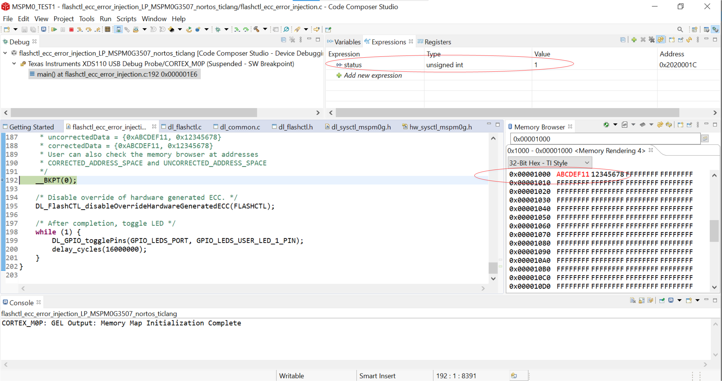
At the second breakpoint, the 64-bit data with the double-bit error triggers a DED (double error detection) error, and the variable status is set as 1. However, the double-bit error is not able to be corrected. The data in the flash aligned with MAIN_BASE_ADDRESS is still the 64-bit data with the double-bit error, this is because a double-bit error is detectable, but not correctable using this form of ECC. Hence why this kind of ECC is called SECDED (single error correction, double error detection) ECC.
Flash ECC Code2#
At the end of the code, the LED status is toggled within the main loop to indicate the program has completed.
See if you can modify the code to see what happens when a triple-bit error occurs. If you get stuck, one possible method is given below. Try a few different 3-bit values in order to ensure you understand whats happening.
Answer for Triple-bit error detection
To keep things simple, we can just change our gDataArray64DED[] or gDataArray64SEC[] value to have 3 different bits from the original data, then run a debug session in CCS with the memory browser open to see what happens. Let’s redo the definition of gDataArray64DED[] like so:
/* Array with "double-bit error" of gDataArray64 */
    uint32_t gDataArray64DED[] = {0xABCDEE11, 0x12345678};
Notice that the value is now different from the gDataArray64[] by 3-bits. If you run the debugger as you did before and watch the memory, you can see if this value is not detected as an error (status=0), or whether it is a single-bit error (status = 2), or a double-bit error (status = 1). You can also see if the erroneous value is corrected, written to memory as is, or if something else happens.
Try this again with a few other three-bit-different values, what happens if you change the first array byte to 0xABCDFF11, 0xABCDEF13, or 0xABCDEF31?
Summary#
At the end of this lab, you should now be able to:
Understand the basic structure of the MSPM0G flash memory
Understand the process of writing and reading to flash memory
Understand the purpose of ECC in flash programming and use ECC to detect and possibly correct writing errors.
Understand how to fully leverage the flash memory in MSPM0.