DRV8706-Q1 EVM GUI User Guide
1. Overview
This graphical user interface (GUI) was developed to allow simple evaluation of a user’s motor with the DRV8706-Q1 evm being controlled by TI’s MSPM0 microcontroller. This guide will go over the key parts of the GUI to allow you to get up and running quickly. You can access the GUI described in this document here.
2. Useful Information
2.1 Hardware Connection.
View the hardware user guide to learn the steps required to get the hardware in the right state to run this GUI example.
2.2 Enabling SPI Communication
The motor driver must not be sleeping (nSLEEP pin is LOW) for SPI communication to work. If you try to perform a SPI write while the motor driver is sleeping the write will fail. Trying to perform a SPI read will likely result in garbage data. If you put the motor driver to sleep for more than 1ms then all the motor driver’s SPI registers will revert to their default value once its out of sleep mode.
2.3 Enabling motor driver output
User must set the DRVOFF pin to LOW as well as set the SPI bitfield IC_CTRL.EN_DRV to 1 to enable gate driver output. As discussed below certain changes in the GUI will automatically have DRVOFF set back to HIGH as a form of protection for the user.
2.4 GUI Protection
The driver mode you select must match how you physically hookup the motor to the DRV8706-Q1 EVM. Therefore, to protect the user any time a driver mode is changed the DRVOFF pin is set high ie the motor driver output is disabled. Even within a driver mode, changing things such as the direction or other settings will either set DRVOFF pin high , duty cycle to 0% or set outputs to HI-Z.
3. Getting Started
To run the demo the user must first follow the steps in the hardware user guide. Then the user must plug the USB cable into the LaunchPad and their computer. Finally they should launch the GUI.
The GUI will automatically program the LaunchPad with the necessary firmware. If everything is successful the bottom left corner of the GUI should say “Hardware connected”.
3. Driver Mode

The DRV8706-Q1 supports different control schemes and this drop down allows you to select between each one. Note by selecting a value in the drop down the motor driver will be automatically configured to use the selected control scheme via SPI operation. Switching between driver modes will result in DRVOFF pin being set high.
3.1 Half-Bridge Mode
Half-Bridge mode allows the user to control two half-bridges independently.
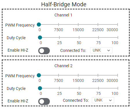
PWM Frequency – Changes the PWM frequency for the given half-bridge
Duty Cycle – Changes the Duty Cycle for the given half-bridge
Enable HI-Z – Will set the corresponding nHIZx pin to LOW which will set the associated motor driver outputs to LOW and high impedance.
Connected To - One of the motor pins needs to be connected to the motor driver’s output pin and the other motor pin needs to be connected to either PVDD or GND. This setting indicates what your connection looks like. Changing this value will automatically enable HI-Z. Leaving this value to UNK will force HI-Z to remain enabled.
Important Note To minimize the number of timers used the LP_MSPM0L1306 HAL module uses one timer for both PWM signals. Therefore, any time you change the PWM frequency for one channel the PWM frequency for the second channel is changed. So you will notice if you change the PWM frequency for Channel 1 the slider for Channel 2 will automatically match it and vice a versa.
3.2 H-Bridge Mode
Configure the DRV8706-Q1 to H-Bridge control mode. This is used to drive a single motor either forward or backward.
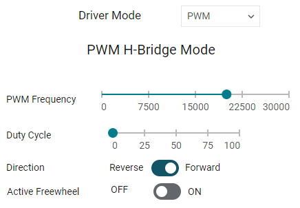
PWM Frequency – Changes the PWM frequency for the given H-Bridge
Duty Cycle – Changes the Duty Cycle for the H-Bridge
Direction – Toggle to change the direction the motor spins. Changing directions will set duty cycle to 0% as a precaution.
Active Freewheel – Toggle to enable Active Freewheel. The determination if this is Low-Side Active Freewheel or High-Side Active Freewheel is determined by the value of the SPI register’s BRG_CTRL.BRG_FW bitfield. The power on reset value is set to use Low-Side freewheeling.
3.3 Phase Enable Mode
Configure the DRV8706-Q1 to Phase Enable Control Mode
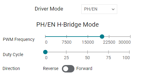
PWM Frequency – Changes the PWM frequency for the given H-Bridge
Duty Cycle – Changes the Duty Cycle for the H-Bridge
Direction – Toggle to change the direction the motor spins. Changing directions will set duty cycle to 0% as a precaution.
3.4 Solenoid Mode
Configure the DRV8706-Q1 to use Solenoid Control Mode
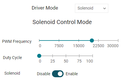
PWM Frequency – Changes the PWM frequency for the solenoid.
Duty Cycle – Changes the Duty Cycle for the solenoid.
Disable/Enable Switch – Toggle if you want to disable or enable the solenoid.
4. Pins Button and Indicators

Controls the state of the MCU’s GPIO output pins connected to the motor driver’s nSLEEP and DRVOFF input pins.
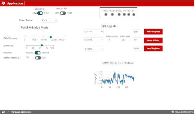
5. Fault Status from SPI Operations
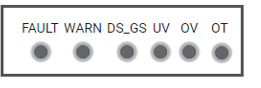
Whenever a SPI read or write operation is performed, the DRV8706-Q1 returns status flags back as part of its response. Grey means the associated motor driver fault hasn’t occurred. Red means the fault has occurred. These status leds are only updated during SPI read or write operations. Note the GUI does not clear any faults automatically so if a fault requires a SPI operation to be cleared the user will have to do so manually.
6. SPI Operations
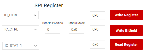
These controls allow you to perform raw SPI operations by clicking on the red button. Note the GUI nor the library performs any protection when performing various SPI operations. So avoid making changes to registers or bitfields that the GUI/library is controlling internally such as the different drive modes.
6.1 Write Register
Performs a SPI write operation based on the register selected and the value specified.
The dropdown selects the SPI register you want to write to.
The input field on the write represents the value you want to write and must include the 0x prefix. Hitting the button writes the value you inputted to the register you selected.
6.2 Write Bitfield
Forms a SPI read modify write operation. This means that you can safely update a register’s bitfield without overwriting other bitfields in the register.
The dropdown selects the SPI register you want to write to.
Bitfield position determines the starting bit. Your mask and value is automatically shifted by the position specified here.
Bitfield mask determines which bits you actually want to modify in hex. Value will be shifted automatically by the bitfield position entered.
The input field on the right represents the hex value you want to write. Value will be shifted automatically by the bitfield position entered.
As an example lets say you want to change CSA_CTRL.CSA_BLK. You want to set it to 75% which means writing 101b. You will set the following
Bitfield Position is 3 since CSA_BLK is from bits 5-3 ie starts at bit 3.
Bitfield Mask is 7 since the max value in the bitfield is 7. So you want to make sure you clear all the bits in this bitfield.
The input field is 0x5 which represents 101b.
6.3 Read Register
The drop down allows you to select which register you want to read.
The input field on the right is read only and will reflect the value that is read.
Anytime you perform a raw SPI write operation the dropdown and input field will automatically match the register you written and show the value that was read back after your write operation has been completed.
7. Current Sense Amplifier Output Voltage

This graph shows the voltage the microcontroller has read from the current shunt amplifier. The plot refreshes with the latest output voltage every 16 ms.