Introduction
Welcome to the MSP430 DAC academy. The DAC module is a voltage-output digital-to-analog converter(DAC). This module can output an analog signal external for control or reference. This academy will demo the usage of DAC in MSP430FR2355.
Prerequisites
Hardware
The following hardware is required for this lab
Software
The following software is required for this lab
Installing the software
NOTE:
The software examples used for this lab should be imported from within the TI Resource Explorer. This can be accessed from the web or locally in CCS by clicking View→Resource Explorer. Before importing a Project, you first need to download MSP430Ware to be able to import the examples to the CCS IDE. This may be done when CCS was installed or can be done later by clicking the "Download and Install" icon in the top right. Note that installing MSP430Ware for any project will install ALL labs and content, so this only needs to be done once.
Recommended Resources
These training materials provide a baseline introduction to the hardware. This documentation can be referenced for the MSP430 MCU and the LaunchPad details.
Overview
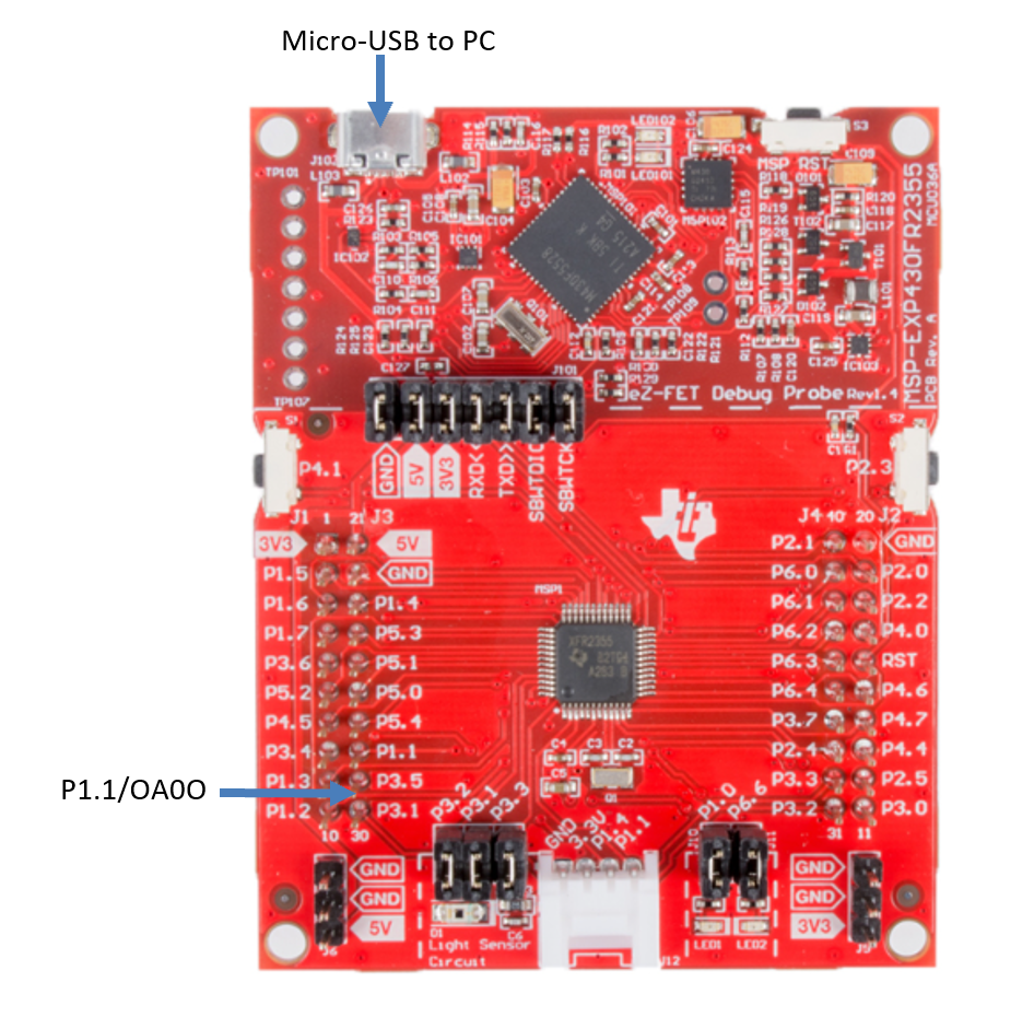
In this academy, we will be using the MSP430FR2355 LaunchPad to enable the MCU's internal DAC, and output a positive ramping voltage on a GPIO pin where it can be measured by a multimeter.
Not all MSP430 families include a DAC and those that do may have different variants. Below is a quick reference table for the different DACs in the MSP430 devices.
| MSP430 Family | DAC module | DAC Features |
|---|---|---|
| FR2xx | SAC | 12-bit, Programmable setup time, Internal or external reference selection, Software selectable data loading |
| F5xx/6xx | DAC12_A | 8-bit or 12-bit voltage-output resolution, Programmable settling time and power consumption, Internal or external reference selection |
| F4xx/FG4xx | DAC12 | 8-bit or 12-bit voltage-output resolution, Programmable settling time and power consumption, Internal or external reference selection |
| F1xx | DAC12 | 8-bit or 12-bit voltage-output resolution, Programmable settling time and power consumption, Internal or external reference selection |
This academy uses MSP430Ware register level code examples from MSP430Ware and the tasks use MSP430FR2355 as an example to show how to output voltage from DAC.
NOTE:
The DAC module and code operation will vary depending on the MSP430 family, so please refer to the code examples respectively.
Getting Started
Hardware Setup:
-
Launchpad Input and Output diagram:
Task – Use the 12 bit DAC to output positive ramp voltage
Example Project Overview
Configure SAC-L3 for DAC Buffer Mode. Use the 12 bit DAC to output a positive ramp. The OA is set in buffer mode to improve DAC output drive strength. The internal 2.5V reference is selected as the DAC reference. Observe the output of OA0O pin with an oscilloscope. ACLK = n/a, MCLK = SMCLK = default DCODIV ~1MHz.
- Import the "msp430fr235x_SAC_L3_05.c" example msp430fr235x_SAC_L3_05.c into CCS from TI Resource Explorer.
MSP430ware→Devices→MSP-EXP430FR2XX_4XX→MSP430FR2355→Peripheral Example→Register Level→
msp430fr235x_SAC_L3_05.cClick import the project into CCS icon at the upper right hand corner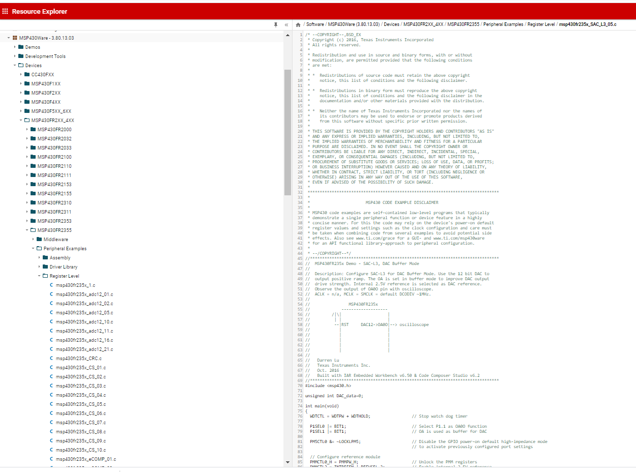
- Build the code and program it to the LaunchPad.
Code Overview and modification
Initialization:
In this code example, the following modules are used: clock system, REF, Timer and SAC.
The Watchdog module should be disabled to prevent the watchdog timer from triggering a reset while the example code is running.
WDTCTL = WDTPW | WDTHOLD; // Stop watchdog timer
Since the code example is using the default clock frequency after power-on, there is no code for clock system configuration.
Default CPU clock is MCLK = SMCLK = default DCODIV ~1MHz. Low frequency peripheral clock ACLK = default REFO ~32768Hz.
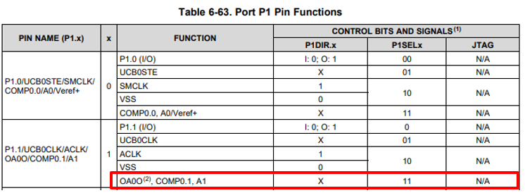
GPIO initialization requires P1.1 be configured as OA0O function. Based on table 6-63 in the datasheet (msp430fr2433 datasheet ), configure register P1SELx to 11.
         P1SEL0 |= BIT1;                           // Select P1.1 as OA0O function
         P1SEL1 |= BIT1;                           // OA is used as buffer for DAC
After GPIO initialization, unlock the GPIO high-impedance mode by resetting the LOCKLPM5 bit. This is needed only for FRAM devices(except MSP430FR57xx family). MSP430 FLASH based MCUs don't need this step.
           // Disable the GPIO power-on default high-impedance mode to activate
           // previously configured port settings
           PM5CTL0 &= ~LOCKLPM5;
Enable internal reference. More details please refer to Reference: Concepts Academy.
          // Configure reference module
          PMMCTL0_H = PMMPW_H;                      // Unlock the PMM registers
          PMMCTL2 = INTREFEN | REFVSEL_2;           // Enable internal 2.5V reference
          while(!(PMMCTL2 & REFGENRDY));            // Poll till internal reference settles
SAC configuration:
This demo uses the SAC0 module configured as a DAC. Two other modules are needed to be configured along with the SAC0: DAC12 and OA. The OA is used to buffer DAC12 output.
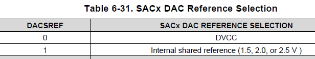
For this DAC12 demo, the internal 2.5 v is selected as the reference and uses TimerB2(TB2.1) to tigger data update event. To select the internal reference as the reference, we need to configure DACSREF to 1 based on table 6-31 SACx DAC Reference Selection in datasheet
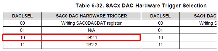
          SAC0DAC = DACSREF_1 + DACLSEL_2 + DACIE;  // Select internal Vref as DAC reference, TB2.1 to triggle output update and enable DAC interrupt
          SAC0DAT = DAC_data;                       // Initial DAC data
          SAC0DAC |= DACEN;                         // Enable DAC
For OA need to be configured as DAC buffer mode as below
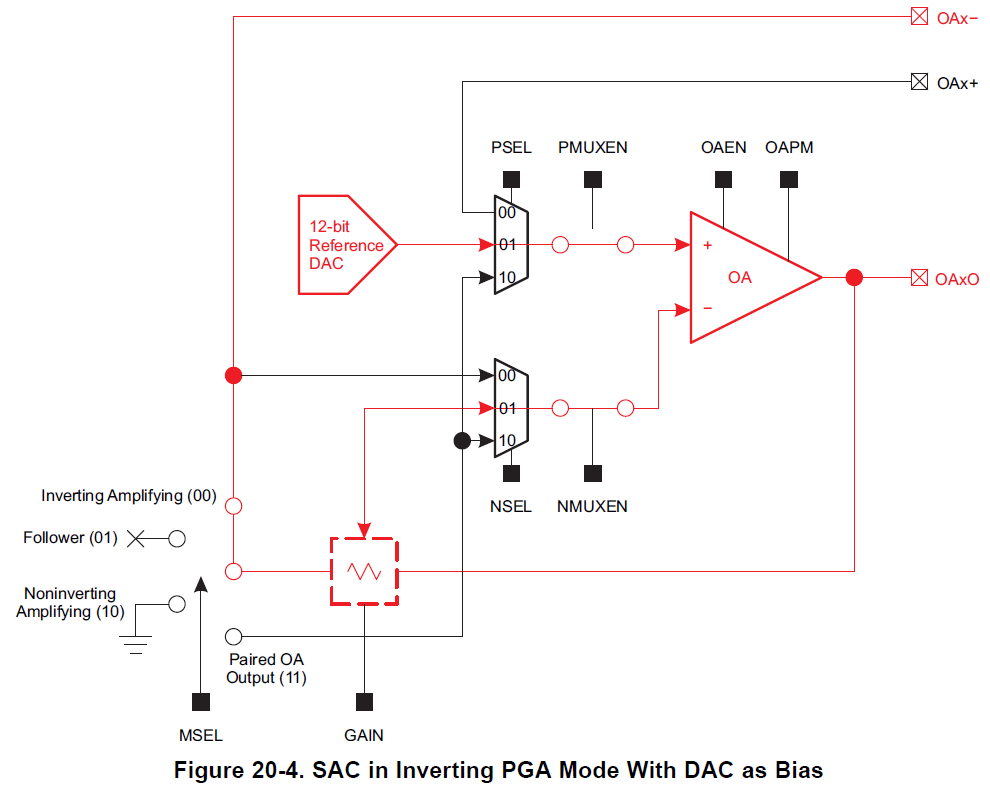
          SAC0OA = NMUXEN + PMUXEN + PSEL_1 + NSEL_1;//Select positive and negative pin input
          SAC0OA |= OAPM;                            // Select low speed and low power mode
          SAC0PGA = MSEL_1;                          // Set OA as buffer mode
          SAC0OA |= SACEN + OAEN;                    // Enable SAC and OA
TimerB configuration:
In this demo, TimerB must be configured in PWM output mode to trigger the DAC value update. More detail about timer configuration, please refer to the Timer: Counter academy. The value update frequency is 1MHz/100 = 10KHz. The timer's configuration code as below.
          // Use TB2.1 as DAC hardware trigger
          TB2CCR0 = 100-1;                           // PWM Period/2
          TB2CCTL1 = OUTMOD_6;                       // TBCCR1 toggle/set
          TB2CCR1 = 50;                              // TBCCR1 PWM duty cycle
          TB2CTL = TBSSEL__SMCLK | MC_1 | TBCLR;     // SMCLK, up mode, clear TBR
Low power mode:
After peripheral configration, put the device into LPM3 and enable global interrupt.
__bis_SR_register(LPM3_bits + GIE); // Enter LPM3, Enable Interrupt
DAC interrupt ISR:
This demo enables the DAC interrupt to upate the new value that will be latched into the SAC0DAT buffer.
            case SACIV_4:
                DAC_data++;
                DAC_data &= 0xFFF;
                SAC0DAT = DAC_data;                 // DAC12 output positive ramp
                break;
Code Execution
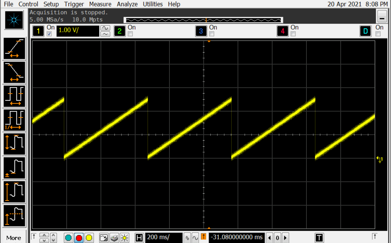
Connect the PC and LaunchPad with a micro USB cable. In CCS, build the example code and program the LaunchPad. After the LaunchPad reset, the code will execute. Connect oscilloscope on pin P1.1.You can see the wave measured below:
What current OA + DAC output load in low power mode with MSP430FR2355?
Summary
At the end of this lab, you should now be able to:
- Understand different DACs in different MSP430 family
- Understand how to configure SAC to DAC mode
This work is licensed under a Creative Commons Attribution-NonCommercial-NoDerivatives 4.0 International License.