Introduction
Welcome to the MSP430 REF academy. Many Analog components, such as ADCs, Comparators, and DACs, need a reference to function properly. Most MSP430s integrate a voltage reference inside the MCU in order to reduce design complexity of your application. This integration comes with the added benefit of reduced external components and board space. This lab demonstrates how to use the MSP430 built-in voltage references module.
NOTE:
For code operation of different reference voltage module in different MSP430 family is different, please refer to the code examples respectively.
Prerequisites
Hardware
The following hardware is required for this lab
Software
The following software is required for this lab
Installing the software
NOTE:
This software examples used for this lab should be imported from within the TI Resource Explorer. This can be accessed from the web or within a locally in CCS by clicking View->Resource Explorer. Prior to Importing a Project, you first need to download MSP430Ware in order to be able to import the examples to the CCS IDE. This may be done when CCS was installed or can be done later by clicking the "Download and Install" icon in the top right. Note that installing MSP430Ware for any project will install ALL labs and content, so this only needs to be done once.
Recommended Resources
These training materials provide a baseline introduction to the hardware. This documentation can be referenced for the MSP430 MCU and the launchpad details.
Overview
This academy will demonstrates how to use the MSP430 built-in voltage references module. You will be using a launchpad and enable the internal voltage reference and then ouput it in the GPIO measure it by multimeter.
Some MSP430 devices can also output the voltage as reference to external components if needed, or accept input from an external reference if an application requires a voltage not provided by the internal reference. The internal reference module varies across MSP430 families as seen in the table below. For the purpose of this lab, we will be focusing on the reference module found in the MSP430FR2433.
| MSP430 Family | Reference module | Output voltage |
|---|---|---|
| FR2xx/4xx | In PMM | External 1.2v, Internal 1.5 v(In enhanced shared reference systems support: 1.5 v, 2.0 v and 2.5 v) |
| FR5xx/6xx | REF_A | 1.2 v, 2.0 v, and 2.5 v |
| F5xx/6xx | REF | 1.5 v, 2.0 v, or 2.5 v (1.2 v just for SD16/24) |
| F2xx/4xx | Internal | 1.5 v or 2.5 v (1.2 v just for SD16/24) |
This lab uses MSP430Ware register level code examples from MSP430Ware.The demo uses MSP430FR2433 as an example to do two tasks:
Task 1: Show how to output the internal voltage reference on Pin 1.4.
Task 2: Show how to use it internal with ADC
Getting Started
Hardware Setup:
-
Launchpad Input and Output diagram:
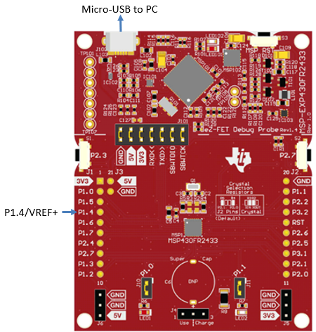
Task 1 – Output the internal reference voltage to outside on Pin 1.4
Example Project Overview
This task will use a simple toggle LED example code "msp430fr243x_1.c" and add few codes to enable internal reference and output it on P1.4
- Import the "msp430fr243x_1.c" example msp430fr243x_1.c into CCS from TI Resource Explorer.
MSP430ware→Devices→MSP-EXP430FR2XX_4XX→MSP430FR2433→Peripheral Example→Register Level→
msp430fr243x_1.cClick import the project into CCS icon at the upper right hand corner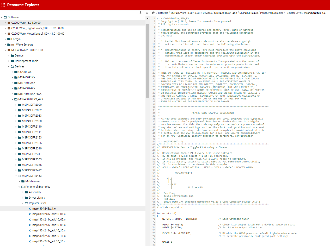
- Build the code and program it to the launchpad.
Code Overview and Modification
Let us break down the MSP430 example code into two parts:
- Initialization
- Main loop
Initialization:
In this code example, following modules are used: Watchdog, clock system and GPIO. These modules need to be configured before the main loop code execution.
The Watchdog module should be disabled to prevent the watchdog timer from triggering a reset while the example code is running.
WDTCTL = WDTPW | WDTHOLD; // Stop watchdog timerSince the code example is using the default clock frequency after power-on, there is no code for clock system configuration.
Default CPU clock is MCLK = SMCLK = default DCODIV ~1MHz. Low frequency peripheral clock ACLK = default REFO ~32768Hz.
GPIO initialization is to configure the package pins to assgined functionalities: GPIO output, REF output. In this example code, port P1.0 is configured to output to toggle LED. P1.4 is used for reference voltage output.
Port pins are often multiplexed with other peripheral module functions. See the device-specific data sheet(msp430fr2433 datasheet ) to determine pin functions. Each port pin uses two bits to select the pin function: I/O port or one of the three possible peripheral module functions. Table 8-3 shows how to select the various module functions. See the device-specific data sheet to determine pin functions. Each PxSEL bit is used to select the pin function: I/O port or peripheral module function. A device in this family may have only PxSEL0 or both PxSEL0 and PxSEL1.
So for P1.0 is used for GPIO,we should configure P1SELx = 00, because the default value of P1SELx is all 0, so we don't need to configure it. To configrue the GPIO output mode, need set first bit in P1DIR register like below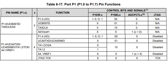
P1OUT &= ~BIT0;    // Clear P1.0 output latch for a defined power-on state
P1DIR |= BIT0;     // Set P1.0 to output direction
After the GPIO initialization, unlock the GPIO high-impedance mode by reset LOCKLPM5 bit. This is needed just for FRAM devices(except MSP430FR57xx family) for flash devices don't need this step.
// Disable the GPIO power-on default high-impedance mode to activate
// previously configured port settings
PM5CTL0 &= ~LOCKLPM5;
Enable reference and output on P1.4
For P1.4 we need to configure it as A4/VREF+ mode we need to configure ADCPCTL4 bit to 1 in register SYSCFG2. And the configuration P1DIR and P1SEL are not cared.
SYSCFG2 |= ADCPCTL4; // Configure P1.4 to ADC A4 pinWhen ADC A4 channel is enabled, the 1.2-V on-chip reference can be output to P1.4 by setting EXTREFEN in PMMCTL2 registers
We need to add the code below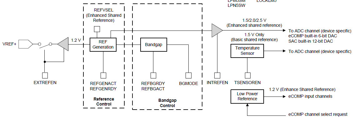
    PMMCTL0_H = PMMPW_H;     // Unlock the PMM registers
    PMMCTL2 |= EXTREFEN;     // Enable output of the reference
    __delay_cycles(400);     // Delay for reference settling
Main loop:
In this code example, the main loop function is simple that just toggle P1.0
         while(1)
         {
           P1OUT ^= BIT0;                      // Toggle P1.0 using exclusive-OR
           __delay_cycles(100000);             // Delay for 100000*(1/MCLK)=0.1s
         }
Code Execution
Connect the PC and launchpad with Micro USB cable. In CCS, build the example code and program the launchpad. After the launchpad reset, the code will execute. You can see the LED1 is togglling. Use multimeter to measue the voltage on Pin1.4 should be 1.2v.
What current limition of the interanl reference when output in MSP430FR2433?
Task 2 – Use internal reference voltage for ADC
Task 2 Overview
This task is the same as task 1 in ADC introduction academy.
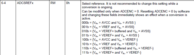
To configure ADC's reference voltage is to set the value of ADCSREFx to 001 in register ADCMCTL0
ADCMCTL0 |= ADCINCH_1 | ADCSREF_1; // A1 ADC input select; Vref is internal 1.5V
The next step is to enable the reference used as internal reference and the code is as below
         // Configure voltage reference for ADC conversion
         PMMCTL0_H = PMMPW_H;          // Unlock the PMM registers
         PMMCTL2 |= INTREFEN;          // Enable internal reference 1.5V
         __delay_cycles(400);          // Delay for reference settling
Summary
At the end of this lab, you should now be able to:
- Understand internal reference voltage in different MSP430 family
- Understand how to output the reference voltage
- Understand how to use the internal reference as ADC's reference
This work is licensed under a Creative Commons Attribution-NonCommercial-NoDerivatives 4.0 International License.