Introduction
This lab introduces the integrated Operational Amplifier(OpAmp) module. It demonstrates the implementation of OpAmp circuits using the MSP-EXP430FR2355 and its integrated Smart Analog Combo(SAC) modules in DAC and Non-inverting PGA modes which can be used in applications requiring signal generation and amplification.
This lab uses register level code examples from MSP430Ware and has 3 tasks consisting of the following activities:
- Setup MCU Opamp in DAC mode with Timer trigger (basic signal generator, modify output)
- Setup MCU Opamp in Non-inverting PGA mode (basic amplifier, modify gain)
- Combine DAC mode OpAmp with Non-inverting PGA mode OpAmp and compare against TINA simulation.
Prerequisites
Hardware
The following hardware is required for this lab
- (1) MSP-EXP430FR2355 LaunchPad
(2) Voltmeter
Optional but recommended to visualize analog signals
(3) Oscilloscope
NOTE:
Although these labs focus on the DC response of MSP430 integrated OpAmps, an oscilloscope is also recommended in order to see the transient response.
Software
- Code Composer Studio (CCS)
- MSP430FR2355 Code Examples
- TINA Simulator
- MSP430FR2355 OpAmp TINA Simulation
- MSP430 Analog Config
Installing the software
NOTE:
The software examples used for this lab should be imported from within the TI Resource Explorer. This can be accessed from the web or locally in CCS by clicking View→Resource Explorer. Before importing a Project, you first need to download MSP430Ware to be able to import the examples to the CCS IDE. This may be done when CCS was installed or can be done later by clicking the "Download and Install" icon in the top right. Note that installing MSP430Ware for any project will install ALL labs and content, so this only needs to be done once.
Recommended Resources
The documentation can be referenced for the MSP430 MCU and the LaunchPad details.
- MSP430FR2355 MCU Datasheet
- MSP430FR4xx and MSP430FR2xx Family User's Guide
- MSP430 MCUs Development Guide Book
- How to Use the Smart Analog Combo in MSP430 MCUs
- What is an OpAmp?
- Getting started with TINA
- Precision Labs OpAmps
Overview
This lab introduces fundamental OpAmp functionality on MSP MCUs.
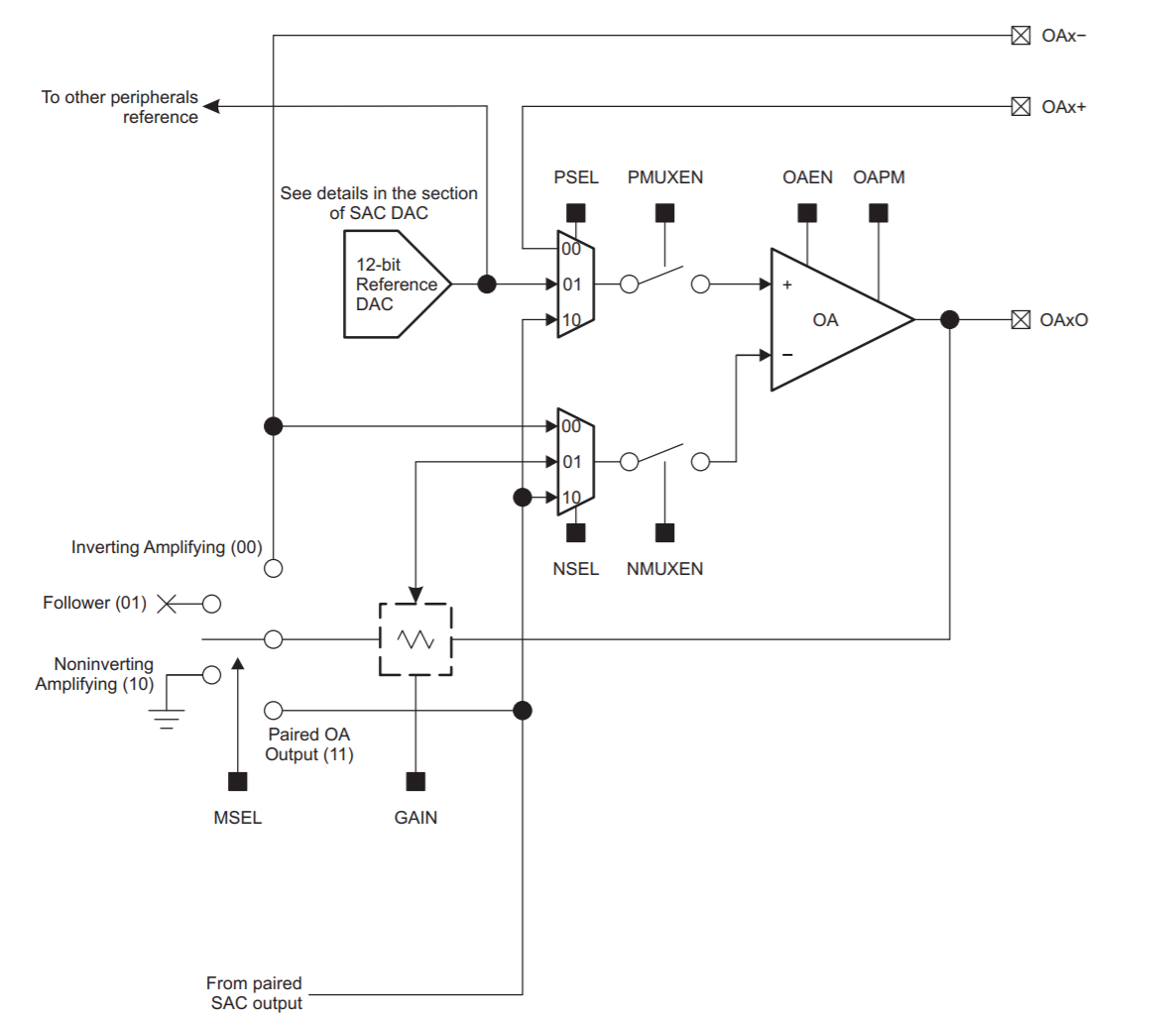
In this lab, you will be using an MSP430FR2355 LaunchPad. Two of the MSP430FR2355 Smart Analog Combos(SAC) will be internally connected together so no external wiring is required. This makes it possible to generate and amplify a signal with no additional hardware required. The architecture of the configurable SAC can be seen in the image below. As can be seen, the inputs to the SAC OpAmp can be configured for an integrated DAC, external pins, programmable gain feedback, or other OpAmp outputs. Each OpAmp can be configured for general-purpose, buffer, DAC, inverting, or non-inverting mode.
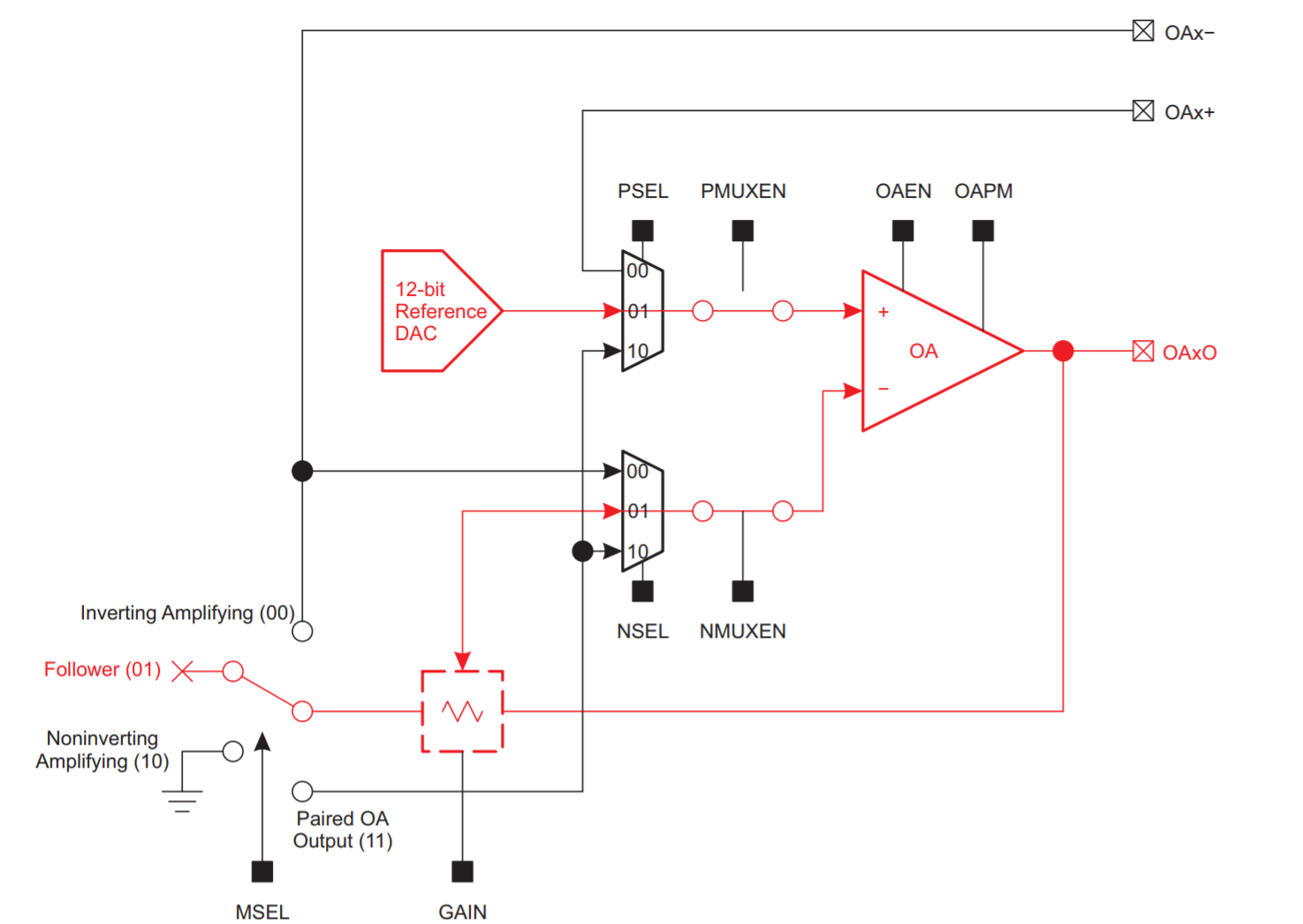
In this lab, we'll be focused on a DAC mode configuration(with OpAmp in follower mode) and a Non-inverting PGA mode configuration. The SAC configurations for DAC mode is depicted below. In this configuration, the DAC output is connected to the positive input of the OpAmp, while the negative input is connected to the output of the OpAmp.
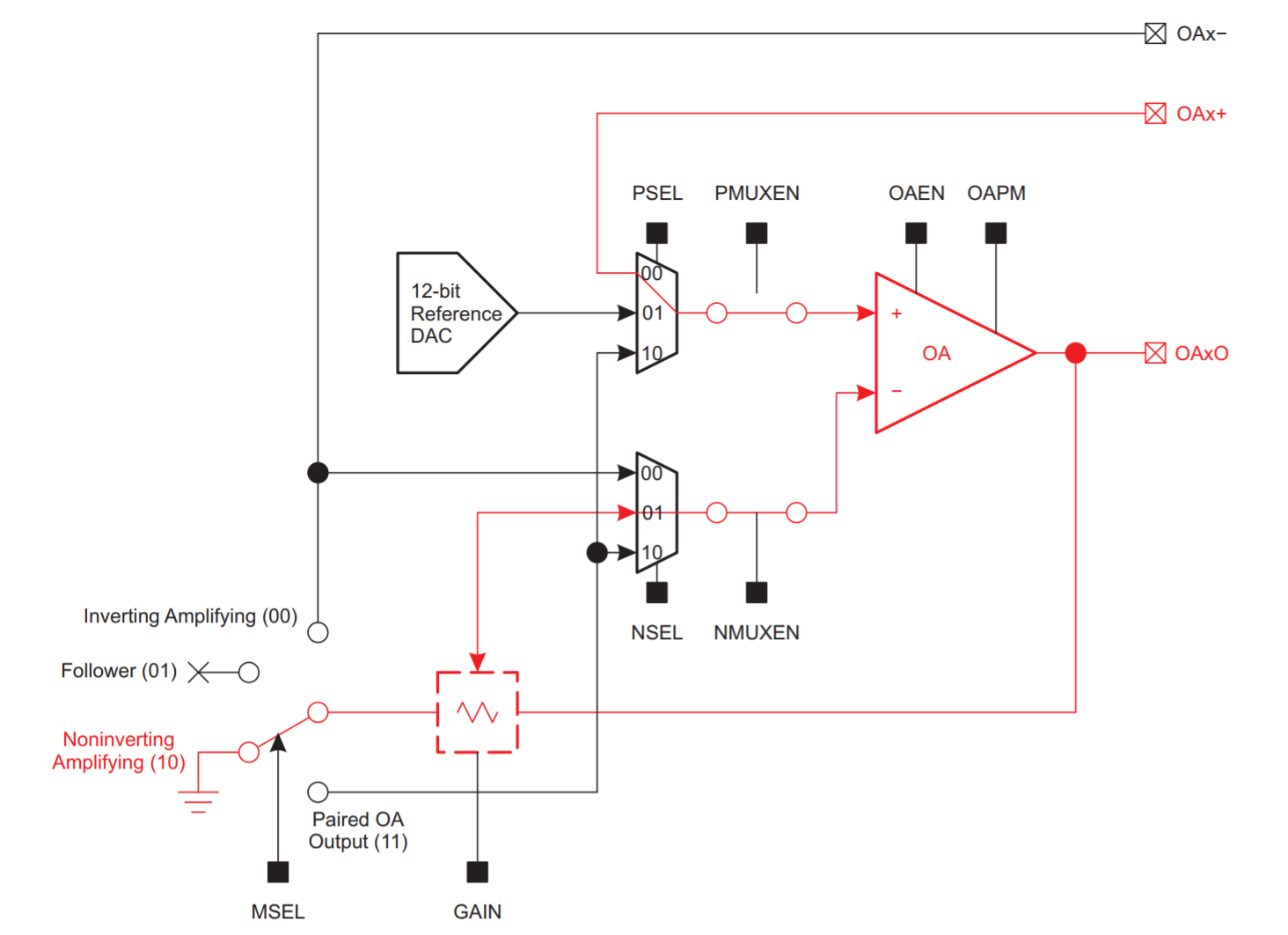
The non-inverting PGA mode SAC configuration is depicted below. In this configuration, the positive input of the OpAmp is connected to an external pin(or another OpAmp) and the negative input of the OpAmp is connected between a feedback resistor and another resistor connected to the ground. The gain of the OpAmp is determined by the resistor values which are configured via the SAC PGA register.
The non-inverting OpAmp configuration is depicted below along with the equation describing the relationship between Vout and Vin. As can be seen, Rf and R2 form a voltage divider for the feedback loop.
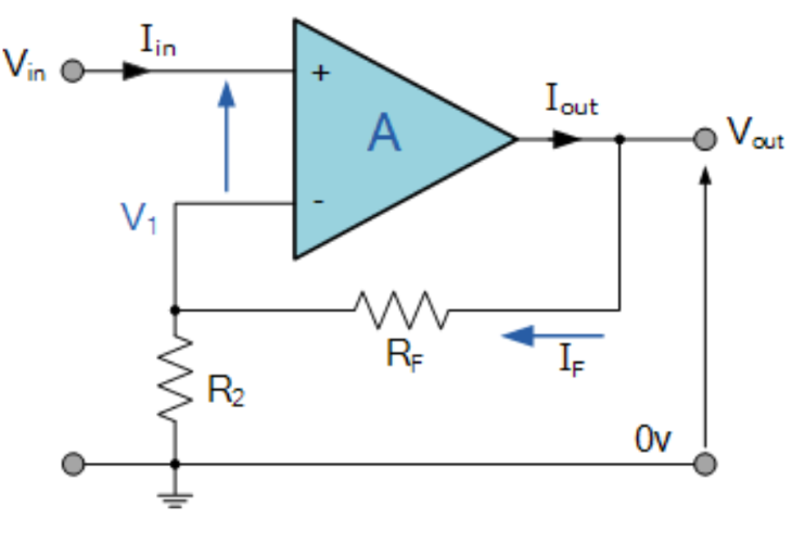
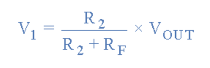
Solving for the ratio of Vout/Vin we get the following for the gain:
To dynamically adjust the gain of this OpAmp for applications requiring Automatic Gain Control(AGC), we can modify the ratio between Rf and Rin via the SAC PGA register to ensure that the amplified output isn't clipped.
Getting Started
Hardware Setup:
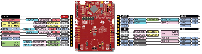
LaunchPad BoosterPack Pinout
Task 1 – DAC Mode Signal Generator
Example Project Overview
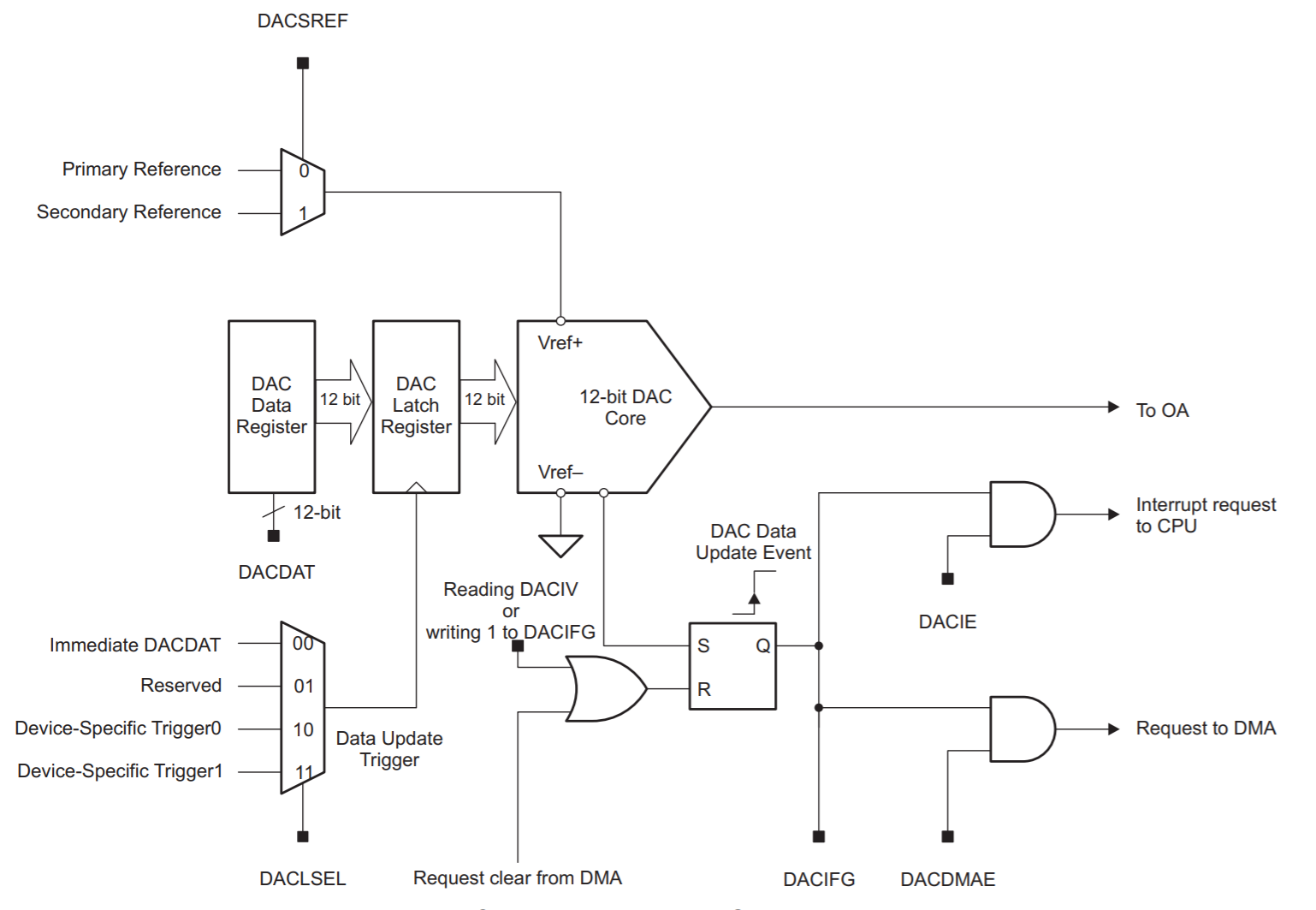
This first project starts with the fundamentals of configuring an OpAmp at the register level and demonstrates how to output a time-varying signal using a Timer trigger. “ To demonstrate OpAmp usage, we need a source signal to feed into the OpAmp. We will be using the internal DAC in this example to fill that role. A timer interrupt is required to periodically update the voltage output by the DAC. As can be seen from the DAC architecture diagram below, the DAC value can be latched by a peripheral(such as a Timer).
For more information about the integrated DAC, please see the DAC: Concepts Academy.
This example demonstrates a ramp signal where the digital value used by the DAC is incremented via an interrupt service routine.
In this task, there is no code to modify, so build and program the MSP430 LaunchPad with the DAC mode example code.
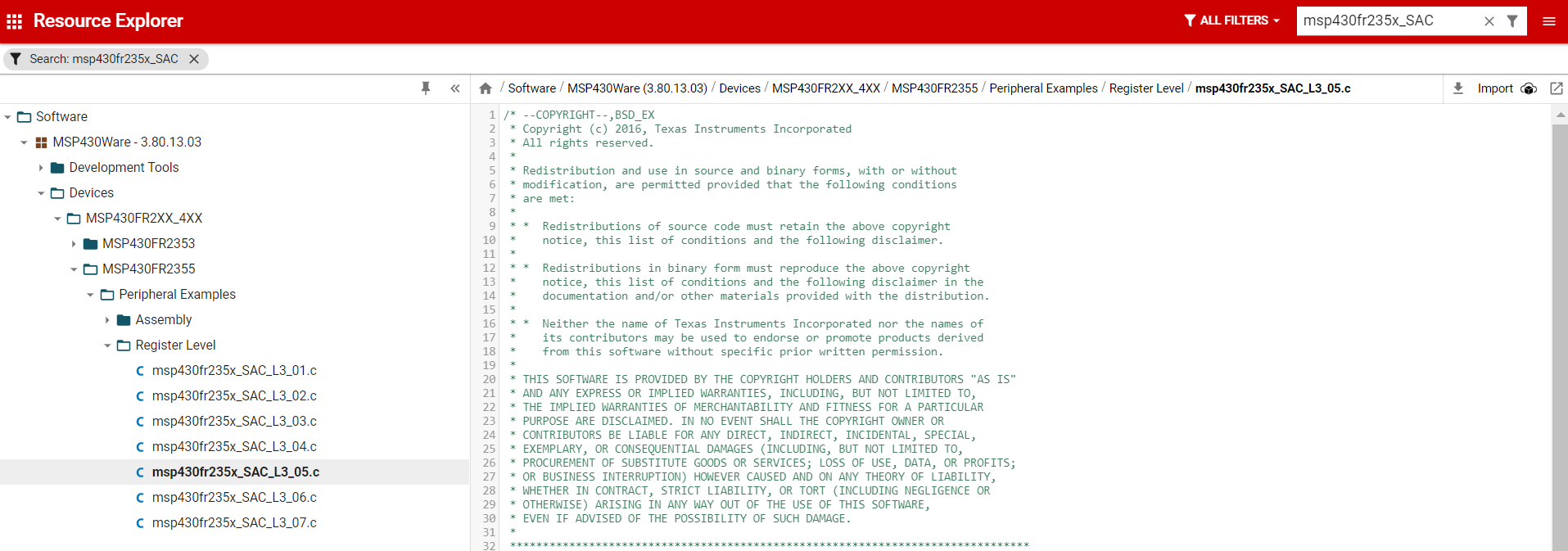
- Import the OpAmp DAC mode example msp430fr235x_SAC_L3_05.c into CCS from TI Resource Explorer.
MSP430Ware→Development Tools→MSP-EXP430FR2355→Peripheral Examples→Register Level→msp430fr235x_SAC_L3_05.c`
- Click Import in the upper right hand corner
- Program the LaunchPad.
- Connect your voltmeter(or oscilloscope) to OpAmp0 output(P1.1) on the Launchpad header.
Code Overview
Let's take a look at the OpAmp and Timer initialization code. Before we setup our OpAmp, we need to configure the reference voltage that will be used. The reference voltage will determine the voltage levels output by the DAC. With a reference voltage of 1.5V, a digital value of 4095 will result in an output voltage of 1.5V. For a reference voltage of 2.5V, the same value will result in an output voltage of 2.5V. The code below sets the internal reference voltage to 2.5V and waits until this voltage settles before proceeding.
    // Configure reference module
    PMMCTL0_H = PMMPW_H;                      // Unlock the PMM registers
    PMMCTL2 = INTREFEN | REFVSEL_2;           // Enable internal 2.5V reference
    while(!(PMMCTL2 & REFGENRDY));            // Poll till internal reference settles
The next portion of the example code configures Smart Analog Combo0(SAC0) which contains an integrated OpAmp and DAC in DAC mode. The internal reference voltage is first selected for the OpAmp0 DAC and the DAC interrupt is enabled. The DAC data is initialized and the DAC for SAC0 is enabled. Both positive and negative inputs to SAC0 are enabled with the OpAmp enabled in low power buffer mode.
    SAC0DAC = DACSREF_1 + DACLSEL_2 + DACIE;  // Select int Vref as DAC reference
    SAC0DAT = DAC_data;                       // Initial DAC data
    SAC0DAC |= DACEN;                         // Enable DAC

    SAC0OA = NMUXEN + PMUXEN + PSEL_1 + NSEL_1;//Select positive and negative pin input
    SAC0OA |= OAPM;                            // Select low speed and low power mode
    SAC0PGA = MSEL_1;                          // Set OA as buffer mode
    SAC0OA |= SACEN + OAEN;                    // Enable SAC and OA
The DAC is updated based on a Timer which is sourced from the MSP system clock (SMCLK) running at 1MHz. This Timer is configured to operate as a PWM with a period of 100 which results in the DAC being updated at a frequency of 10kHz. After setting up the OpAmp and Timer, the DAC is updated based on the Timer's Capture Compare Register reaching a count of 50.
     // Use TB2.1 as DAC hardware trigger
     TB2CCR0 = 100-1;                           // PWM Period/2
     TB2CCTL1 = OUTMOD_6;                       // TBCCR1 toggle/set
     TB2CCR1 = 50;                              // TBCCR1 PWM duty cycle
     TB2CTL = TBSSEL__SMCLK | MC_1 | TBCLR;     // SMCLK, up mode, clear TBR
The interrupt service routing for SAC0 has a case (SACIV_4) which is triggered by the timer. In this code, the DAC data is updated to produce a ramp signal.
     case SACIV_4:
     DAC_data++;
     DAC_data &= 0xFFF;
     SAC0DAT = DAC_data;                 // DAC12 output positive ramp
     break;
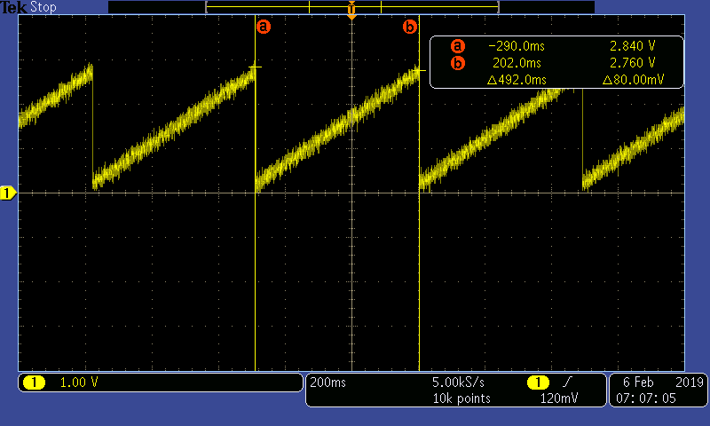
With your voltmeter(or oscilloscope), you should see a ramp signal with a frequency slightly greater than 2Hz.
Because most voltmeter's won't update fast enough to see this ramp function, you can modify the code above to update the SAC0DAT register with a constant value of 1500. This should result in a DC voltage around 0.9V on P1.1.
To check your understanding so far, let's take a quick quiz.
In the example provided, what would be the expected output voltage of the DAC with a 2V reference and a digital value of 2048?
Task 2 – Non-inverting Mode PGA
Example Project Overview
In this task, the code example demonstrates how to configure an OpAmp in Non-inverting mode.
Once you get the example code working with your PC, your goal will be to reconfigure the OpAmp to change the gain on the fly.
This modified example will be needed in the next task that follows.
- Import the Non-inverting Mode PGA code example msp430fr235x_SAC_L3_04.c from Resource Explorer.
MSP430ware→Development Tools→MSP-EXP430FR2355→Peripheral Examples→Register Level→MSP430FR2355→
msp430fr235x_SAC_L3_04.c- Click import in the upper right hand corner
- Program the LaunchPad.
- Connect your voltmeter(or oscilloscope) to OpAmp0 output(P1.1) on the Launchpad header.
Code Overview
Let's take a look at the OpAmp initialization code. This code configures the OpAmp in SAC0 to operate in Non-inverting PGA mode with a gain of 17.
    SAC0OA = NMUXEN + PMUXEN + PSEL_0 + NSEL_1;//Select positive and negative pin input
    SAC0OA |= OAPM;                           // Select low speed and low power mode
    SAC0PGA = GAIN0 + GAIN2 + MSEL_2;         // Set Non-inverting PGA mode with Gain=17
    SAC0OA |= SACEN + OAEN;                   // Enable SAC and OA
You can quickly confirm that the OpAmp is working by connecting a jumper between P1.3 and GND or 3.3V on the platform. While checking the output on P1.1 with a voltmeter. Next, reduce the gain setting to 2 by removing "GAIN2" from the code above.
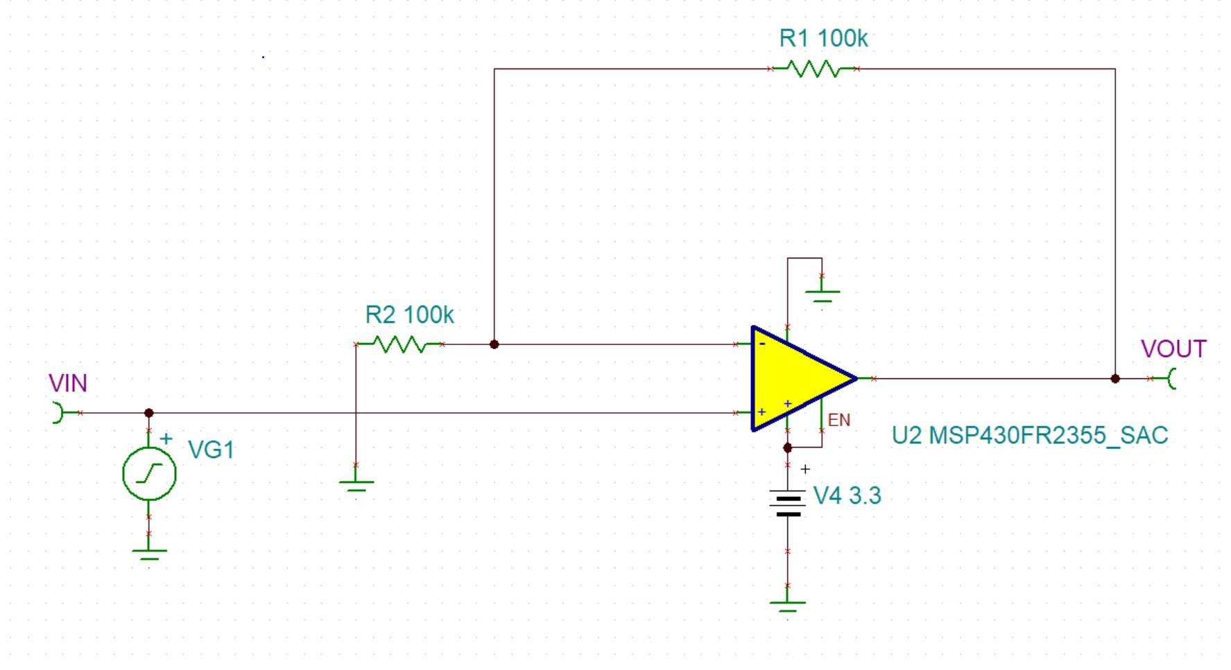
Next we'll look at a TINA simulation of what we would expect to see with this OpAmp in Non-inverting PGA mode. In this simulation, we'll first modify the OpAmp configuration to reflect a Non-inverting configuration with a gain of 2. Your modified simulation should look like the image below.
Next, you'll need to configure the input signal (VG1) to output a triangle wave with DC offset of 1.25V and peak to peak amplitude of 2V. Once you've done this, you should select Transient under the Analysis menu and click OK. The output should look like below:
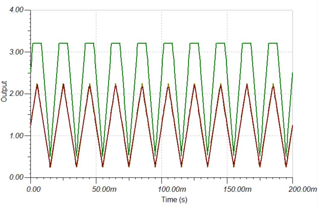
As can be seen, the signal is amplified to 2x of the input until we get close to 3.3V because the OpAmp is powered by a 3.3V supply. In this task, we were able to configure an SAC OpAmp for Non-inverting PGA mode with a gain of 2 and modify a model to simulate what we might expect to see with an triangular wave input.
Task 3 – DAC Mode Signal Generator/Non-inverting PGA Combination
In this portion of the lab, you will build on what you learned in the last two tasks by modifying the DAC mode OpAmp code example to work with a different OpAmp which can then feed its output into the Non-inverting PGA mode OpAmp input implemented in the previous task. Once this is implemented, we will look at the differences between the output produced by this implementation versus the TINA simulation implemented in task 2.
There are 3 actions that need to be performed:
- Modify the existing DAC Mode OpAmp Code Example to work with a different OpAmp module.
- Modify the existing Non-inverting PGA Mode OpAmp Code Example to take the input from this different OpAmp module.
- Compare the TINA simulation against the platform results.
Software Modifications
Changing the OpAmp Module
Each OpAmp module will use a similar set of configuration registers. The primary difference is with regards to the muxing of inputs and outputs. Change the DAC mode OpAmp to use SAC2 instead of SAC0 in the example. Build the example and connect your voltmeter to P3.1 to confirm that you are seeing a voltage around 0.9V on P3.1.
Connecting the output of one OpAmp to the input of a second OpAmp
Different OpAmp cascading configurations are possible without external wiring for different architectures. SAC2 and SAC0 can be connected internally on the MSP430FR2355 by changing the PMUX or NMUX selection of SAC0.
Here is a hint showing how to change the SAC0 OpAmp input MUX to take it's input from SAC0:
SAC0OA = NMUXEN + PMUXEN + PSEL_2 + NSEL_1;
Non-Inverting Mode TINA Simulation vs. Platform Results
Once you've implemented your combined DAC Mode Signal Generator/Non-inverting PGA Mode Combo you should connect your voltmeter(or oscilloscope) to P1.1 to compare the response of your Non-inverting OpAmp for comparison with your TINA simulation. You might notice that there is a slight difference between platform voltage and simulation results when inputting a DC voltage. This could be due to a small input offset voltage which can be calibrated for on these devices. When providing the ramp signal to your Non-inverting PGA, you should seem something like this:
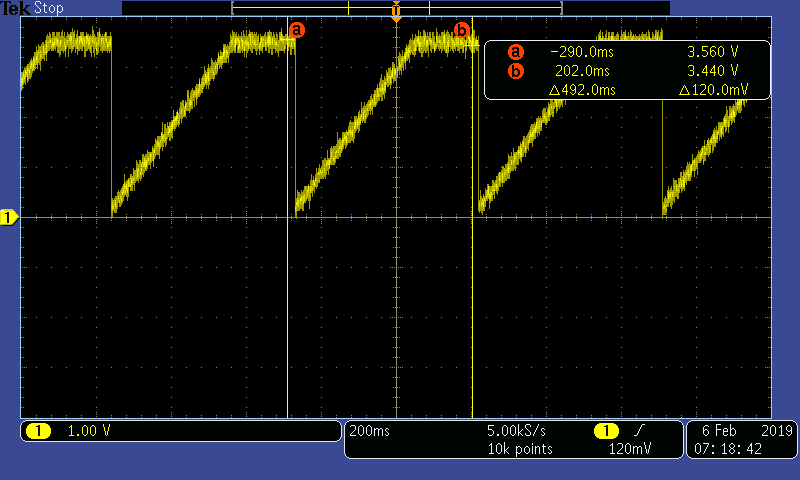
As expected from the simulation, the output is also clipped around 3.3V.
To check your understanding so far, let's take a quick quiz.
In this task, why is there a difference seen between the TINA simulation and the platform DC response at different voltages?
Perform Some Useful Action
Now that you have a simple Non-inverting PGA, how can it be made more useful? For many applications, it's desirable to maintain the amplitude of the amplified signal despite variations in the amplitude of the input signal over a given period of time. This is referred to as Automatic Gain Control(AGC). If we know the periodicity of the input signal, it's possible to implement AGC by looking for the peak of the signal over a capture period. In order to do this, well need some additional code to periodically capture the ADC signal such as:
// Configure ADC12
ADCCTL0 |= ADCSHT_2 | ADCON;                             // ADCON, S&H=16 ADC clks
ADCCTL1 |= ADCSHP;                                       // ADCCLK = MODOSC; sampling timer
ADCCTL2 &= ~ADCRES;                                      // clear ADCRES in ADCCTL
ADCCTL2 |= ADCRES_2;                                     // 12-bit conversion results
ADCIE |= ADCIE0;                                         // Enable ADC conv complete interrupt
ADCMCTL0 |= ADCINCH_1;                                   // A1 ADC input select; Vref=AVCC
ADCCTL0 |= ADCENC | ADCSC;                               // Sampling and conversion start
with an Interrupt Service Routing to capture the results after conversion such as:
// ADC interrupt service routine
#if defined(__TI_COMPILER_VERSION__) || defined(__IAR_SYSTEMS_ICC__)
#pragma vector=ADC_VECTOR
__interrupt void ADC_ISR(void)
#elif defined(__GNUC__)
void __attribute__ ((interrupt(ADC_VECTOR))) ADC_ISR (void)
#else
#error Compiler not supported!
#endif
{
    switch(__even_in_range(ADCIV,ADCIV_ADCIFG))
    {
        case ADCIV_NONE:
            break;
        case ADCIV_ADCOVIFG:
            break;
        case ADCIV_ADCTOVIFG:
            break;
        case ADCIV_ADCHIIFG:
            break;
        case ADCIV_ADCLOIFG:
            break;
        case ADCIV_ADCINIFG:
            break;
        case ADCIV_ADCIFG:
            ADC_Result = ADCMEM0;
            __bic_SR_register_on_exit(LPM0_bits);            // Clear CPUOFF bit from LPM0
            break;
        default:
            break;
    }
}
Challenge
Congratulations on making it to the end! Now, if you are up to the challenge, think about how you might modify your AGC code to adapt to input signals which have time varying amplitudes at some known frequency. In order to quickly evaluate other possible OpAmp configurations with your platform, please download the MSP430 Analog Config utility.
Summary
At the end of this lab, you should now be able to:
- Have a fundamental understanding how integrated OpAmps can be configured for signal generation and amplification.
- Have a working understanding of the differences seen between TINA simulation and platform results for MCU integrated OpAmps.
- Re-configure OpAmps for different input and output connections.
- Make a working AGC Non-inverting PGA.
This work is licensed under a Creative Commons Attribution-NonCommercial-NoDerivatives 4.0 International License.