Introduction
Welcome to the MSP430 Timer compare academy. This academy introduces the basics of using the Timer_A module in compare mode to generate pulse-width modulated (PWM) waveforms with variable period and duty cycles and is demonstrated on a MSP-EXP430FR2433 LaunchPad.
Prerequisites
Hardware
The following hardware is required for this lab
- MSP-EXP430FR2433 LaunchPad
- 1 female-to-female Jumper wire
Software
Installing the software
NOTE:
This software examples used for this lab should be imported from within the TI Resource Explorer. This can be accessed from the web or within a locally in CCS by clicking View->Resource Explorer. Prior to Importing a Project, you first need to download MSP430Ware in order to be able to import the examples to the CCS IDE. This may be done when CCS was installed or can be done later by clicking the "Download and Install" icon in the top right. Note that installing MSP430Ware for any project will install ALL labs and content, so this only needs to be done once.
Associated academies
These academies cover using the timer in different modes as well as provide additional information on the timer functionality.
Recommended Resources
The Precision Labs training videos series provides baseline introduction to the timers and clocks. The documentation can be referenced for the MSP430 MCU and the LaunchPad details.
- TI’s Precision Lab Videos: Clocks and Timing
- MSP430FR2433 MCU Datasheet
- MSP430FR4xx_2xx MCU UserGuide
- MSP-EXP430FR2433 Launchpad User's Guide
- MSP430 MCUs Development Guide Book
Overview
In this academy you will be using the MSP430FR2433's Timer_A module to learn how timer modules works in MSP430 MCUs. There are a few versions of timer modules in MSP430 devices that may have varying features (such as Timer_B), however Timer_A is a very good representation of the MSP430 Timer architecture.
Each timer academy will review example code to show how to initialize necessary I/O pins, clocks, and configure Timer_A for its specified purpose, and include instructions for you to modify the provided example as well as quiz questions to check your understanding.
For initial introduction to Timer_A features, please see the Timer: Counter Academy Timer: Counter Mode. In this academy we detail the compare features of the Timer_A module for generating waveforms.
Timer_A Compare Introduction:
Timer_A is a 16-bit timer/counter with up to seven capture/compare registers (CCRx). Timer_A can support multiple captures or compares, PWM outputs, and interval timing. Timer_A also has extensive interrupt capabilities. Interrupts may be generated from the counter on overflow conditions and from each of the capture/compare registers.
The 16-bit timer/counter has two operation modes, capture or compare, and three counting modes: Up Mode, Continuous Mode, and Up/Down Mode. This academy focuses on using the timer in compare mode with the timer running in up mode.
Compare Mode
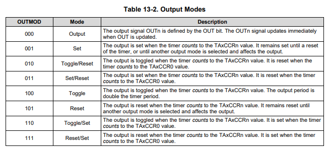
The compare mode is selected when the control register bit CAP = 0 in the TAxCCTLn Register (Timer_Ax Capture/Compare Control n Register). The compare mode is used to generate PWM output signals or interrupts at specific time intervals. Each capture/compare register (CCRx) can drive an output, which can be used to control a GPIO directly. There are several output modes which can be used to generate signals, in this case PWM waveforms. The outputs are controlled by their associated CCRx registers, for example Timer_A1's output 1 (TA1.1) is tied to the CCR1 in the timer module. Each output has eight different output modes, controlled out OUTn bits, that define the behavior of the output when the timer counts to the value specified in associated TAxCCRn register.
The biggest difference between using these outputs in compare mode, vs maunally toggling the GPIO like was done in the Timer: Counter Mode Academy., is that these outputs are controlled automatically by the timer. The CPU is not needed and is not interrupted or worken up, so it can remain asleep or continue doing other tasks.
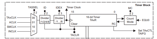
Timer Output in Up Mode
In up mode, there are two points in time when the output signal can change. First is when the timer counts up to the TAxCCR0 value and rolls back to zero. In up mode, TAxCCR0 is used to set the period for your PWM. The second is when the timer count hits the value in the outputs CCRx register, and this is typically used to set your duty cycle of the PWM. The below figure shows an example using for TAx.1, controlled by TAxCCR1.
The most commonly used output modes, especially for generating PWMs, are Mode 3: Set/Reset and Mode 7:Reset/Set.
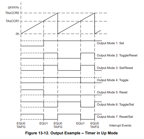
The output mode settings supported on Timer_A are detailed below:
For output timing diagrams in continuous mode and Up/Down mode, please see the Timer_A Chapter of the MSP430FR4xx_2xx MCU UserGuide.
Note: Updating TAxCCRn registers
The timer should be stopped by writing the MC bits to zero (MC = 0) before writing new data to TAxCCRn. Updating TAxCCRn while the timer is running could result in unexpected behaviors.
Getting Started
Hardware Setup:
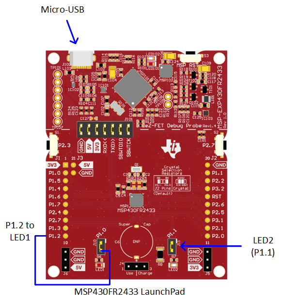
- Plug in the MSP-EXP430FR2433 LaunchPad into your PC using a Micro-USB cable.
Remove the P1.0 jumper (J10) and connect P1.2 to LED1 with a jumper wire. Make sure the P1.1 jumper is populated to connect LED2.
Task 1 – Run Compare mode example and modify it
In this task we will generate two PWM waveforms with variable duty cycles on pins 1.1 and 1.2, connected to LEDs on the MSP430FR2433 launchpad. We will introduce using Timer_A in compare mode to generate PWMs and also go over how to use Timer clock dividers.
Import the timer example
- Import the Timer_A 16 example msp430fr243x-ta0-16.c
into CCS from TI Resource Explorer.
MSP430ware→Devices→MSP430FR2XX_4XX→MSP430FR2433→Peripheral Examples→Register Level→
msp430fr243x-ta0-16.c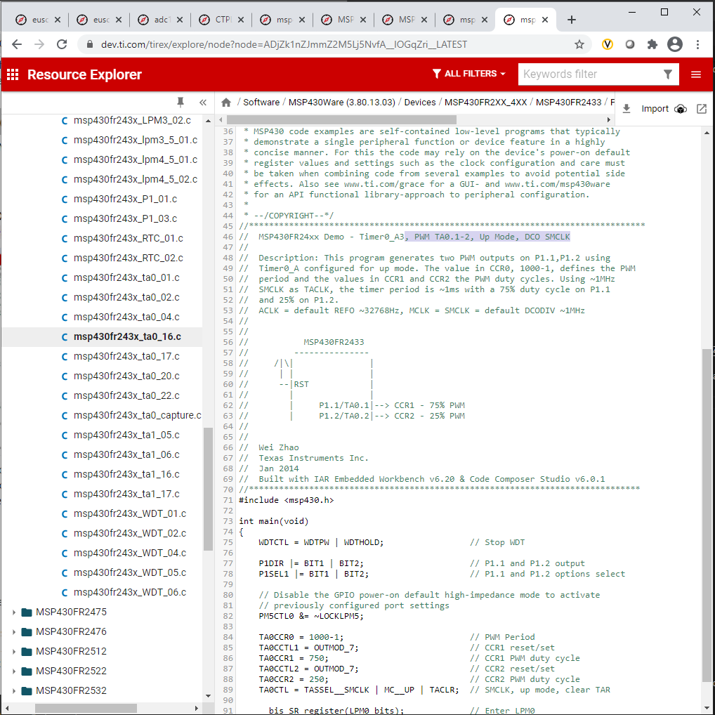
- Click import in the upper right hand corner
- Download and run the example on the launchpad, you should see both LEDs light up.
- You can't see it with your eyes, but both LEDs are actually blinking very quickly.
Code Overview
MSP430 Initialization
Before configuring the MSP430's Timer_A module, we need to initialize the MSP430 by
disabling the watchdog timer and initializing the GPIO pins as outputs from the Timer_A0 to drive the LEDs. The watchdog timer
must be stopped to prevent the MCU from reseting while the demo is running. We will output PWM waveforms directly
from Timer_A using TA0.1 and TA0.2, which are multiplexed to pins 1.1 and 1.2. These pins must be configured to
be connected to the timer, and this is done using the direction register (P1DIR) and selection registers (P1SELx) according
to Table 6-17 of the MSP430FR2433 datasheet.
    #include <msp430.h>

        int main(void)
        {
        WDTCTL = WDTPW | WDTHOLD;             // Stop WDT

        P1DIR |= BIT1 | BIT2;                 // P1.1 and P1.2 output
        P1SEL1 |= BIT1 | BIT2;                // P1.1 and P1.2 options select

        // Disable the GPIO power-on default high-impedance mode to activate
        // previously configured port settings
        PM5CTL0 &= ~LOCKLPM5;

            ...

        }
Timer PWM Period
Now, we can initialize the Timer_A module. In this example, the timer will be configure for compare mode using up mode. This means
that the timer counts until TA0R it reaches the value in the TA0CCR0 register, then on the next count will loop back to 0. This
means that TA0CCR0+1 will be the PWM's period (extra count is for rollover to 0.)
In this example, the TA0CCR0 is set to 999.
TA0CCR0 = 1000-1; // PWM Period
Further down, the clock is configured to SM_Clk which is running at 1MHz. This mean our period is:
PWM Period = (TA0CCR0 + 1) / Timer freq. = (999 + 1) / 1 MHz = 1 ms
PWM Frequency = 1 / PWM Period = 1 / 1 ms = 1 kHz
Timer PWM Duty Cycle
Duty cycle of a PWM is the ratio of time the signal is high vs the time it's low. So, before we can understand how to control the duty cycle, we must understand how the output will interact with the timer. This is controled by the output modes, described in the Timer_A Introduction section.
    TA0CCTL1 = OUTMOD_7;                      // CCR1 reset/set
    TA0CCR1 = 750;                            // CCR1 PWM duty cycle
This example configures TA0.1 by setting TA0CCTL1 to Output Mode 7: Reset/Set, which means that when the timer counter starts restarts at 0 the output is set 'high' and
when the timer hits TA0CCR1 the output goes low for the remaining period. In this case, we known that the output will be high from 0 to 750, then low from 751 to 1000. this
means TA0.1 will have a duty cycle of 75%.
Duty Cycle = Period High / Total Period = 750 / 1000 = 75%
TA0.2 is configured basically the same.
    TA0CCTL2 = OUTMOD_7;                      // CCR2 reset/set
    TA0CCR2 = 250;                            // CCR2 PWM duty cycle
What is the duty cycle for TA0.2?
Timer Start
Next, we can set the timer clock source to SMCLK (1 MHz default), then clear and actually start the timer in up mode using the TA0CTL register. Finally,
the CPU can be put in low power mode for the rest of the time because the PWM outputs are being driven directly from the timer.
    TA0CTL = TASSEL__SMCLK | MC__UP | TACLR;  // SMCLK, up mode, clear TAR

    __bis_SR_register(LPM0_bits);
    __no_operation();
Which of these is NOT a step to configure a PWM output on TA0.1?
PWM Outputs
Now let's see some of the PWM waveforms in action!
- Luckily, P1.1 (
TA0.1) is shared with LED2 (Green LED) on the LaunchPad as long as the P1.1 jumper is connected. It should appear 'ON' now and fairly bright because the LED is blinking at 1 kHz at 75% duty cycle.- If you change the duty cycle to 25% and reprogram the board, this will make the LED appear much dimmer compared to 75%.
- P1.2 (
TA0.2) should be connected to LED1 (Red LED) via a jumper wire and should also be 'ON' but dim.
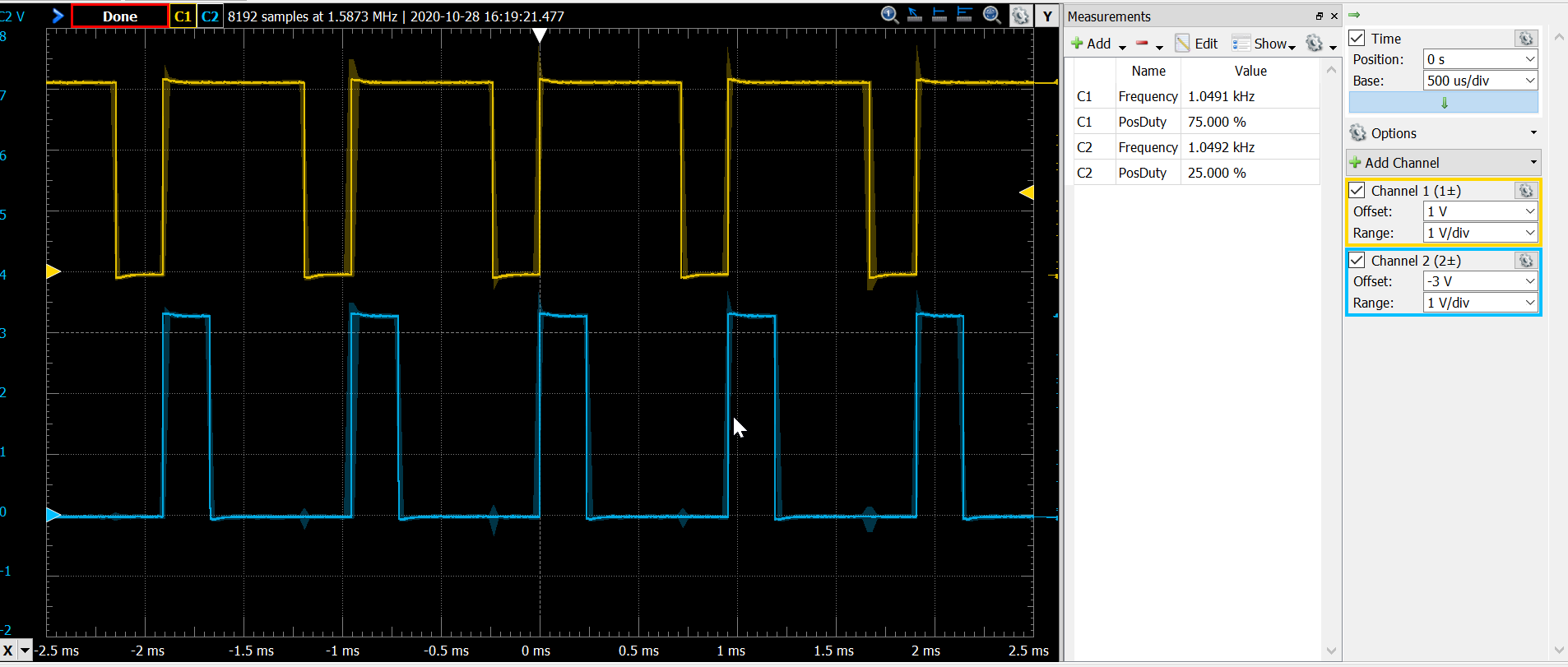
The oscilloscope screenshot below shows the PWM waveforms measured on P1.1 and P1.2. The frequency is ~1 kHz with 75% and 25% duty cycles respectively.
Blink the LED at 32 Hz.
Finally, let's slow the clock down significantly so that we can really see the PWM waveforms visually.
Lights appear "on" to the human eye at 60 Hz or greater, so let's reduce the PWM frequency from ~1 kHz to under 60 Hz. As decribed in the Timer counter lab, you can use ACLK (~32.678 kHz) rather than SMCLK (~1 MHZ) as the clock timer source. With TA0CCR0 = 1000, this would result in a PWM frequency of 32.678 kHz / 1000 = 32.678 Hz.
Change the clock source from SMCLK to ACLK in the TA0CTL register and see the difference:
TA0CTL = TASSEL__ACLK | MC__UP | TACLR; // SMCLK, up mode, clear TAR
You may see the LED very subtly blink off, but the LED still appears mostly "ON" because it is still blinking over 30 times a second!
Changing PWM Frequency to 1 Hz
Finally, let's slow the clock down significantly so that we can really see the PWM waveforms visually. LEDs appear "on" to the human eye at 60 Hz or greater, so let's reduce the PWM frequency from ~1 kHz to under 60 Hz. In this case, let's slow down to 1Hz. This way, we can actually observe the PWM period and duty cycle.
As decribed in the Timer counter academy, you can use ACLK (~32.678 kHz) rather than SMCLK (~1 MHZ) as the clock timer source and the timer's clock dividers to slow the timer's clock and achieve much slower PWM frequencies.
In this case, we are going to stick with the 1MHz SMCLK as our input source, but we are going to use Timer_A's built in clock dividers introduced in the Timer Counter Academy. We first need to figure out how much we need to divide the clock. Since Timer_A is only 16 bits, our max count for the period is 65,535. So to achieve a 1 second period, we need to to be under 65.535 kHz.
We have two 1-8x dividers available on Timer_A: ID (input divide) Attribution-NonCommercial-NoDerivatives IDEX (input divide extended). If we divide the SMCLK/8 = 1MHz/8 = 125kHz. We will still need to divide further. If we take the 125 kHz / 8 = 15.625 kHz. Perfect!
So, how do we configure the dividers? If you search in the datasheet, you will find that the ID bits can be found in the TA0CTL reigster and the TAIDEX bits live in a the TA0EX0 register. We need to configure these when we initialize our timer. Here is what that looks ilke in software:
TA0EX0 = TAIDEX_7;                                    // TAIDEX_7 is dividing the clock by 8
TA0CTL |= TASSEL__SMCLK | ID__8 | MC__UP;               // SMCLK/8,  UP mode
Note:
Remember to configure IDEX first, since when we configure ID__8 we also start the timer by putting it in continuous mode and we don't want to switch the clock source while the timer is running.
What do we need to set CCR0 to for a 1 second PWM period?
Great! But, since we changed out Timer period count, we also need to adjust our duty cycle for both outputs.
To keep 75% duty cycle for TA0.1, what should we set CCR1 to?
What should CCR2 be to keep TA0.2 at a 25% duty cycle?
Great! Now update the code and program the board. When you run it, you should see both LEDs blinking once a second. The green LED2 is tied to the 75% duty cycle TA0.1 and the red LED1 is connected to TA0.2. So, you should see the green LED on much longer than the red LED. If now, check the solution below.
This is what these changes look like in software. You can copy and paste this solution if you would like to replace your Timer Initialization code.
TA0CCR0 = 15625-1;                        // PWM Period
TA0CCTL1 = OUTMOD_7;                      // CCR1 reset/set
TA0CCR1 = 11719;                          // CCR1 PWM duty cycle
TA0CCTL2 = OUTMOD_7;                      // CCR2 reset/set
TA0CCR2 = 3906;                           // CCR2 PWM duty cycle

TA0EX0 = TAIDEX_7;                        // TAIDEX_7 is dividing the clock by 8
TA0CTL |= TASSEL__SMCLK | ID__8 | MC__UP; // SMCLK/8,  UP mode
By switching the timer clock source to ACLK, the timer will run at ~32.768 kHz instead of the 1MHz from SMCLK. As seen on the SMCLK tab, this input clock can be slowed down further using the built in clock dividers and/or we can adjust the CCR0 and CCR1 registers for this new clock frequency. Since our PWM period is already 1000 counts, if we can divide ACLK down to 1 kHz, then we don't need change any of the CCRx settings.
Luckily, we can divide the 32.768 kHz clock by 32, to achieve running the timer at roughly 1 kHz. To
do this, we can use TA0EX0 to divide the clock by 4, and set ID__8 in TA0CTL to divide
the clock by a further ratio of 8.
This results in a new clock frequency of 32.678 kHz / 32 = ~1 kHz, and a new PWM frequency of 1 kHz / 1000 = 1 Hz!
    TA0EX0 = 3;                               // divide by 4
    TA0CTL = TASSEL__ACLK | MC__UP | ID__8 | TACLR;  // ACLK, up mode, clear TAR, div by 8
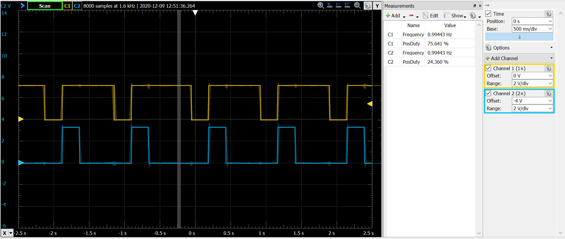
Execute the code and you should really be able to see how slow the LED is blinking now. Try changing the TA0CCR1 value to get PWM duty cycles of 25% or lower and see the visual effect on the LED. The waveforms below show the new PWM waveforms with a 1 Hz frequency at 75% and 25% duty cycles.
What are ways to slow down the PWM frequency and increase the PWM period?
Summary
At the end of this Academy you should now be familiar with:
- Generate PWM waveforms using Timer_A compare mode in up mode using the CCRx registers
Use the Timer input clock to generate correct PWM frequencies and duty cycles

This work is licensed under a Creative Commons Attribution-NonCommercial-NoDerivatives 4.0 International License.