|
xWRL684x MMWAVE-L-SDK
06.00.05
|
|
|
xWRL684x MMWAVE-L-SDK
06.00.05
|
|
The millimeter wave demo (Mmwave_demo) is the out of box (OOB) millimeter wave radar signal processing chain demo on xWRL684x SOC device. This chapter presents the millimeter wave demo (mmwave_demo) radar signal processing chain demo implementation details on xWRL684x SOC device using the MMWAVE LP SDK. The chapter provides a description of the signal processing flow. It also focuses on the implementation details of the low-level signal processing chain. The processing chain is based on range-doppler detection.
| Parameter | Value |
|---|---|
| CPU + OS | r5fss0-0 freertos |
| Toolchain | ti-arm-clang |
| Board | xWRL6844-evm |
| Example folder | examples/mmw_demo/mmwave_demo |
To flash and visualize the OOB Demo see Running the Demo using Visualizer
A GUI tool SysConfig is used to configure different modules and peripherals of the example. Using this tool, users can select and customize different modules and peripherals. The SysConfig tool will generate the code for initializing and configuring these modules. This configuration is saved to a file called example.syscfg for every example. To know more about how to use SDK with SysConfig, Visit this page
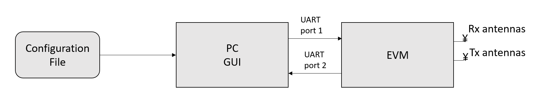
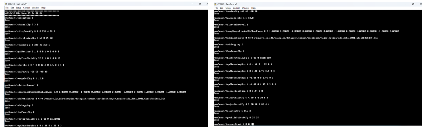
The demo detection demo setup is shown in Figure below. The demo configuration is provided by the command line interface (CLI) configuration file. The PC visualizer is connected to xWRL684x EVM board via a two UART ports. Initially, to start a demo, a set of CLI configuration commands is sent to the EVM. Based on the configuration the EVM sends through the different port various detection information to the visualizer, such as point cloud, range profile, and stats data.
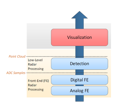
The processing layers of the demo is shown below
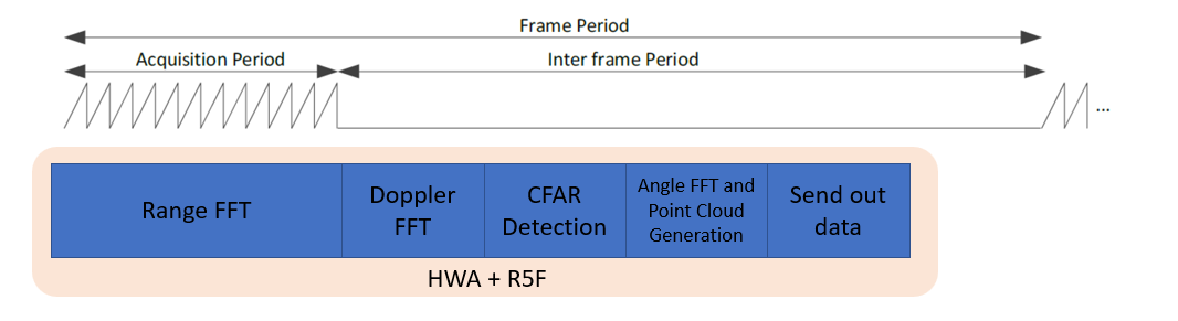
Below is the top-level radar signal processing timing diagram per frame
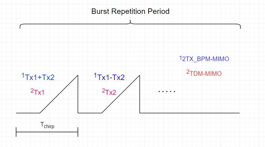
To achieve full MIMO capabilities, the xWRL6844 demo uses one of three demodulation techniques: 2TX_BPM-MIMO, 4TX_BPM-MIMO, and TDM-MIMO. Following sections briefly summarize the modulation schemes.
Typical timing diagram for 2TX-TDM and 2TX-BPM is illustrated in Figure below.
Typical timing diagram for 4TX-TDM and 4TX-BPM is illustrated in Figure below.
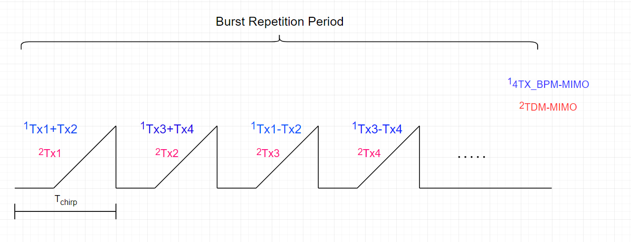
In the TDM-MIMO scheme, only one TX antenna is active in a given chirp, and all the TX antennas are enabled in the frame in an alternating manner. For example, for 4 TX (TX1, TX2, TX3, and TX4), chirp 0 has only TX1 enabled, chirp 1 has only TX2 enabled, chirp 2 has only TX3 enabled, chirp 3 has only TX4 enabled, chirp 4 has only TX1 enabled, and so on. Therefore, no additional demodulation step is needed in the TDM-MIMO scheme because the chirps from the TX antennas are separated in the time domain and stored in the radar cube properly.
Similar to TDM-MIMO, in the BPM-MIMO scheme, a frame consists of multiple blocks. However, unlike in TDM-MIMO, where only one TX antenna is active per chirp interval, two transmit antennas are active in each chirp interval. For the 2TX_BPM-MIMO depicted in Figure above, in the even time slots (0, 2, ...), both transmit antennas are configured to transmit with positive phase, i.e. (TX1, TX2) = (+, +). In the odd time slots (1, 3, ...), the transmit antennas are configured to transmit with phase (TX1, TX2) = (+, -). And for the 4TX_BPM_MIMO, the time slots (0,4, …), TX1 and TX2 are configured to transmit with positive phase, i.e. (TX1, TX2) = (+, +). The time slots (1,5, …), TX3 and TX4 are configured to transmit with positive phase, i.e. (TX3, TX4) = (+, +). The time slots (2,6, …), TX1 and TX2 are configured to transmit with phase (TX1, TX2) = (+, -). And the time slots (3,7, …), TX3 and TX4 are configured to transmit with phase (TX3, TX4) = (+, -).
Therefore, when the BPM mode is enabled, the signal processing chain must decode the received chirp pairs to separate the transmission from each TX antenna. In the current demo BPM demodulation (if enabled) is done as part of the aoa2d DPU.
Let TX1 and TX2 represent chirp signals from two TX antennas in 2TX_BPM-MIMO. In time slot zero, a combined signal SA= TX1+TX2 is transmitted. Similarly, a combined signal SB= TX1-TX2 is transmitted in time slot one. Using the corresponding received signals (SA and SB) at a specific received RX antenna, the components from the individual transmitters are separated using
With simultaneous transmission on both TX antennas, the total transmitted power per chirp interval is increased, and it can be shown that this translates to an SNR improvement. On the other hand, the average power consumption also increases with the BPM-MIMO mode compared to the TDM-MIMO scheme.
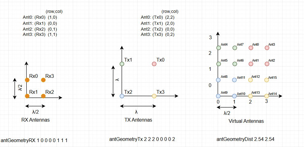
The mmWave demo can support different antenna configurations. Antenna geometry, range bias and phase compensation can be defined using either the antGeometryBoard CLI command or all four of the antGeometryTx, antGeometryRx, antGeometryDist and compRangeBiasAndRxChanPhase ClI commands. Refer to Sensor front-end parameters for more details.
The antenna spacing, antenna indices and the virtual antenna array are shown in Figure below. The right-most figure shows the virtual antennas. For calculating the TX/RX indices(row,col) for antGeometryTx/antGeometryRx, left bottom antenna is considered at origin and lamda/2 is considered for 1 unit in co-ordinate system.
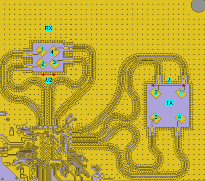
Below figure shows the antenna configuration on the xWRL684x EVM board.
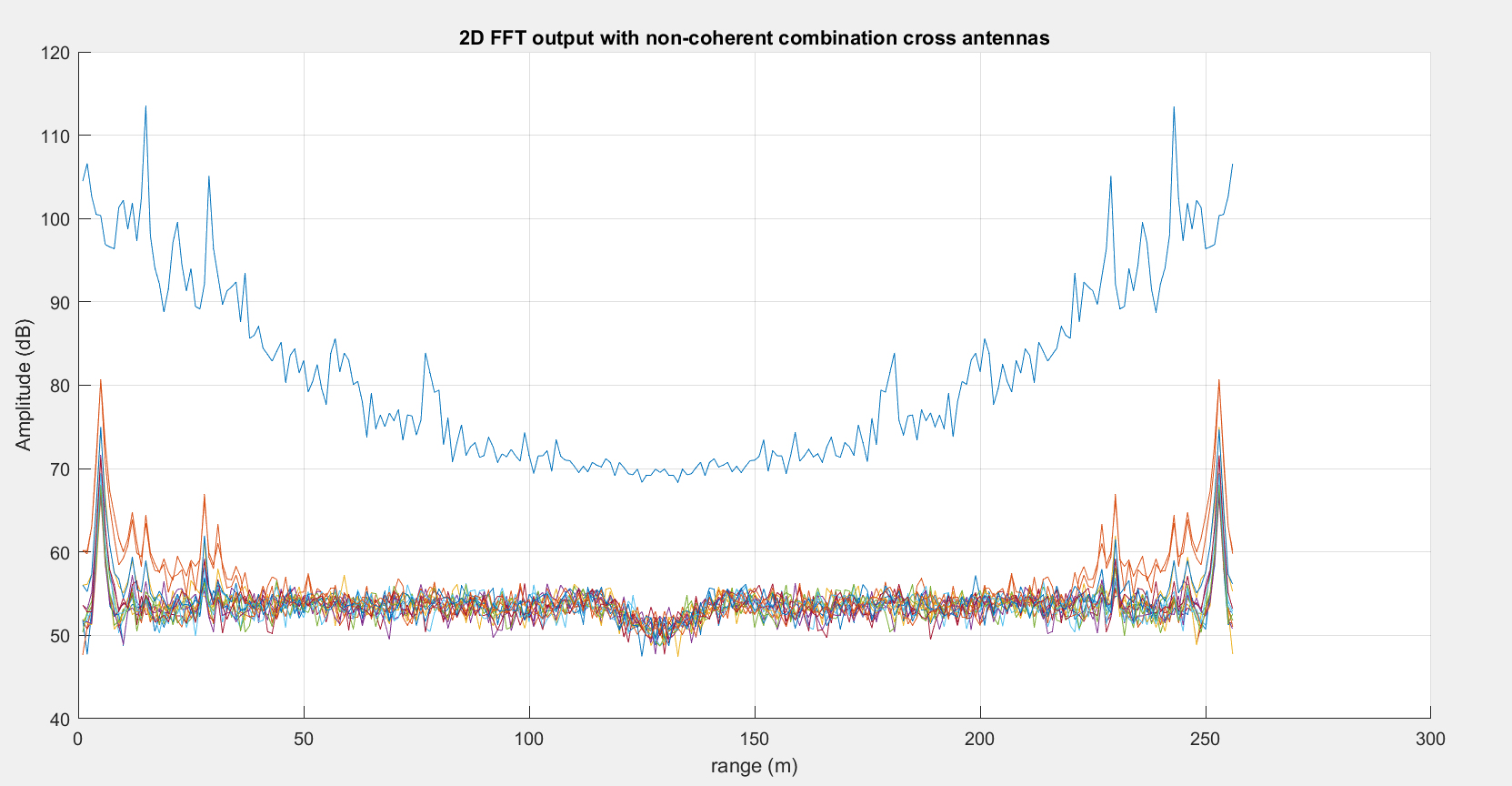
The top-level view of this signal processing chain is shown in Figure below. This chain performs object detection in dange-doppler detection matrix.
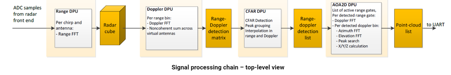
The signal processing consists of the following data processing units:
Because of imperfections in antenna layouts on the board there is a need to calibrate the sensor to compensate for bias in the range estimation and the receive channel gain and phase imperfections. The demo provides the ability to do the measurement and compensation.
The measurement procedure is configured using a CLI command measureRangeBiasAndRxChanPhase. The following is the command syntax:
measureRangeBiasAndRxChanPhase {enabled} {targetDistance} {searchWindow}
The procedure is implemented by the function mmwDemo_rangeBiasRxChPhaseMeasure(). It is called in the processing chain after the range processing DPU. The input to the procedure is a radar cube. The measurement procedure first calculates the range profile as the sum of the magnitude squares across all antennas on the range FFTs. Then it searches for the peak in the zone 𝑋−𝐷/2 ≤ 𝑟𝑎𝑛𝑔𝑒 ≤ 𝑋+𝐷/2 where 𝐷 = searchWindow and 𝑋 = targetDistance.
The procedure then estimates the peak position using the three point parabolic interpolation and the range bias as the difference between the peak position and the configured target distance X.
The Rx channel compensation coefficients are calculated according to following equations.
From the radar cube stored as a complex16 3D array 𝑋[𝑟𝑎𝑛𝑔𝑒][𝑐ℎ𝑖𝑟𝑝][𝑎𝑛𝑡𝑒𝑛𝑛𝑎], the received symbols are extracted at the range index 𝑖𝑝𝑒𝑎𝑘 of the peak position corresponding to the target as
The coefficients are calculated as
where
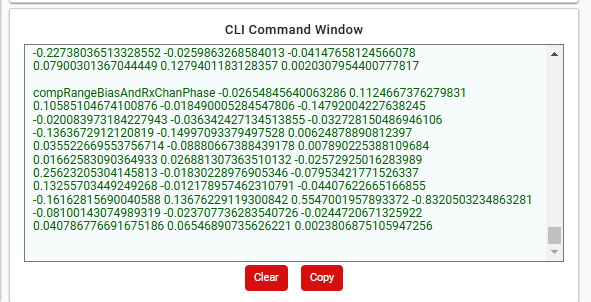
The coefficients are sent per frame to the host within the TLV packet.
Measurement Procedure Steps:
This demo is implemented on xWRL684x using multiple tasks running in the system. Below shows the task flow and tasks used in the system.
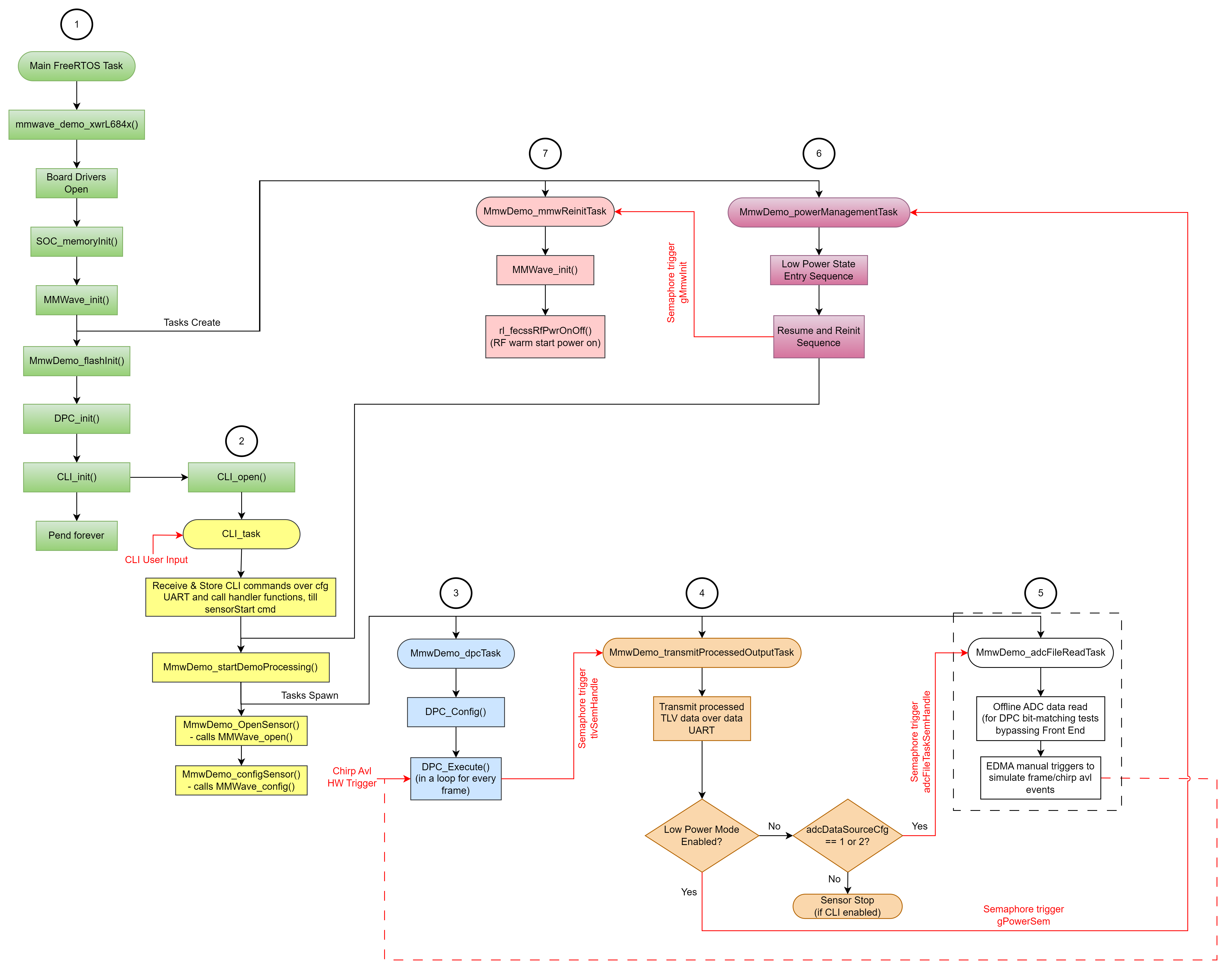

This is free RTOS main task initially called by the main function. It is active only during the start time, and after the creation of the CLI task it rests in pending state.
The CLI task provides the execution context for the command line interface. It includes simple command parser.
The DPC task provides the execution context for the detection processing chain.
This task controls the transfer of radar detection data to the host. The task transmits one packet of data per radar frame using a TLV format structure. Depending on the CLI configuration command guiMonitor the task sends point cloud, range profile, detection matrix, etc.
This task is used for running the unit tests for the demo. The task reads reference ADC data samples from the file and feeds the signal processing chain instead of real ADC data coming from the RF
This task is engaged when the demo is running in the power saving deep sleep mode.
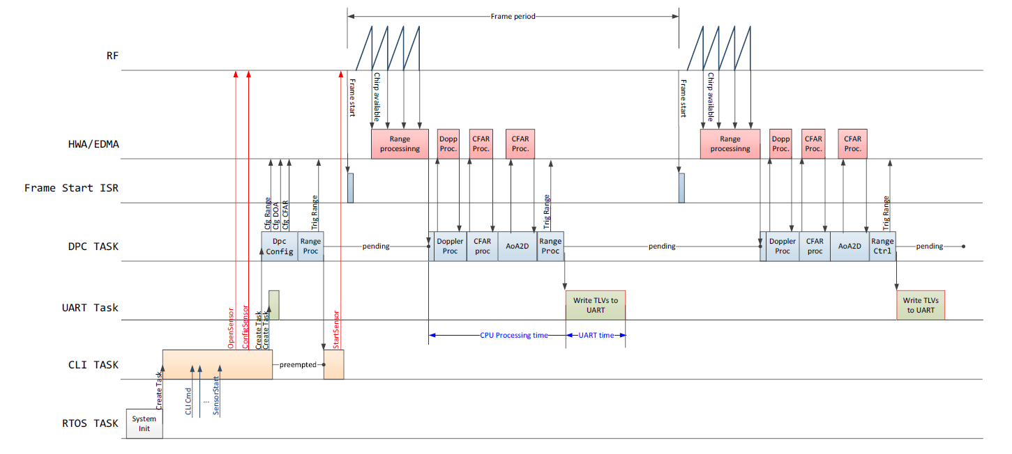
The timing diagram during the startup and the first two frames is illustrated in Figure below.
The timing diagram in the low power mode is shown below.
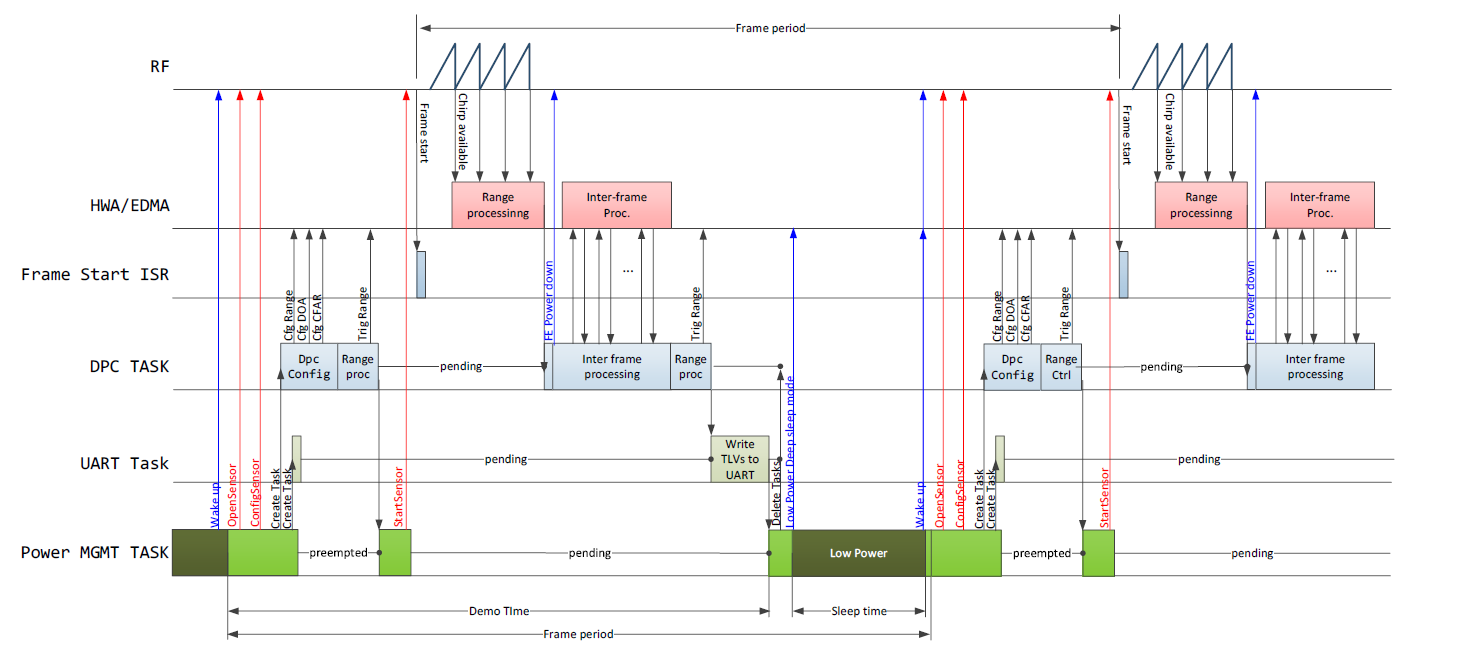
Currently the CPU time and the UART transmit time is reported to Host within the stats TLV. The explanation of these time intervals is shown in the timing diagram above.
Each line in the .cfg file describes a command with parameters. The various commands and their arguments are described in the table below (arguments are in sequence)
| Commands | Parameters | Notes |
|---|---|---|
| sensorStop | Reserved | Default value: 0 NOTE: This command(sensorStop 0) stops the sensor from transmitting further frames. |
| channelCfg | RxChCtrlBitMask | In this field, when bits 0, 3, 4 and 7 are set to 1, they activate the Rx1, Rx2, Rx3 and Rx4 antennas respectively. Some of the combinations are as shown : RX antennas 1,2,3,4 mask = 0x10011001b = 153(decimal) RX antennas 1 and 2, mask = 0x00001001b = 9(decimal) RX antennas 2 and 3, mask = 0x00011000b = 24(decimal) RX antennas 1, 2 & 3, mask = 0x00011001b = 25(decimal) and so on |
TxChCtrlBitMask | In this field, setting bits 0 and 1 to 1 activates Tx1, bits 2 and 3 to 1 activate Tx2, bits 4 and 5 to 1 activate Tx3, and bits 6 and 7 to 1 activate Tx4. Some of the combinations are as shown: TX antennas 1,2,3,4 mask = 0x11111111b = 255(decimal) TX antenna 1,2,3 mask = 0x111111b = 63(decimal) TX antenna 2,3 mask = 0x111100b = 60(decimal) and so on | |
Reserved | Default value: 0 NOTE: This is reserved for future use. | |
| chirpComnCfg | DigOutputSampRate | Digital output Sampling rate for chirp ADC samples. Digital sampling rate is given by 200MHz/ DigOutputSampRate. |
DigOutputBitsSel | Digital output sample bits select, this field governs which bits of the FECSS DFE's internal 16 bit signed data path are sent as output. 0 - Digital sample output is 12 MSB bits of DFE after rounding 4 LSBs 1 - Digital sample output is 12 bits after rounding 3 LSBs & clipping 1 MSB 2 - Digital sample output is 12 bits after rounding 2 LSBs & clipping 2 MSB 3 - Digital sample output is 12 bits after rounding 1 LSBs & clipping 3 MSB 4 - Digital sample output is 12 LSB bits after clipping 4 MSB 5 - Digital sample output is 16 bits | |
DfeFirSel | The final stage FIR filter's characteristics can be selected as below. 0 - Long Filter (90% visibility): This provides visibility to a larger range of IF frequencies: 0 to 0.45 x Sampling Rate. Beyond that, the filter response starts drooping & enters filter transition band. 1 - Short Filter (80% visibility): This provides faster settled outputs but the IF frequency range visible is 0 to 0.40 x Sampling Rate. Beyond that, the filter response starts drooping & enters filter transition band. | |
NumOfAdcSamples | No. of ADC samples. Valid Range: 2 to 1024 | |
ChirpTxMimoPatSel | 1 - TDM pattern 4 - BPM pattern Note: 2TX or 4TX BPM demodulation is performed based on TX channels selected in channelCfg cmd. For more info refer MIMO Modulation Schemes | |
ChirpRampEndTime | Chirp Profile Ramp end Time. This is a common ramp end time value for all chirps in a frame. | |
ChirpRxHpfSel | Chirp Profile HPF corner frequency. This is a common HPF corner frequency value for all chirps in a frame. 0 - 175kHz HPF corner frequency 1 - 350kHz HPF corner frequency 2 - 700kHz HPF corner frequency 3 - 1400kHz HPF corner frequency | |
| chirpTimingCfg | ChirpIdleTime | Chirp Profile Idle Time. This is a common idle time value for all chirps in a frame. Unit: 1us. |
ChirpAdcSkipSamples | Chirp Profile ADC start skip samples. This is a common adc start time value for all chirps in a frame | |
ChirpTxStartTime | Chirp Profile TX start Time. This is a common TX start time value for all chirps in a frame.This field indicates the TX start time in the chirp cycle with respect to the knee of the ramp. Unit: In usec | |
ChirpRfFreqSlope | Chirp Profile RF Frequency Slope. This is a common RF frequency slope value for all chirps in a frame.This field indicates the required FMCW slope of the chirp. Unit: MHz/us Valid range:- 399MHz/us to +399MHz/us. | |
ChirpRfFreqStart | Chirp Profile RF start Frequency. This is a common RF start frequency value for all chirps in a frame. This field indicates the required start frequency of the chirp. Unit: GHz | |
| frameCfg | NumOfChirpsInBurst | Number of Chirps in a Burst. This field indicates the number of chirps to be generated per burst. NOTE: The maximum supported total number of chirps(NumOfChirpsInBurst * NumOfBurstsInFrame) is 1024 when 4 Rx antennas are enabled. |
NumOfChirpsAccum | Number of accumulation per chirp. This field indicates the Number of chirps to be accumulated before sending the ADC data out in DFE, this can be used to increase the SNR without increasing the number of chirps to process in the DSP/HW accelerator. | |
BurstPeriodicity | Burst periodicity in μs. This field indicates the period of the burst. | |
NumOfBurstsInFrame | Number of bursts per frame. NOTE: The maximum supported total number of chirps(NumOfChirpsInBurst * NumOfBurstsInFrame) is 1024 when 4 Rx antennas are enabled. | |
FramePeriodicity | Frame Periodicity. This field indicates the period of the frame, 32bit counter.This field indicates the frame periodicity, the time gap between successive frame starts. Unit: ms | |
NumOfFrames | Number of frames. Valid range: 0 to 65535, 0 means infinite | |
| gpAdcMeasConfig | channelEnable | GPADC channels ON/OFF control, 1 bit per channel. bit[0] corresponds to GPADC channel 0, bit[1] corresponds to GPADC channel 1, bit[2] corresponds to GPADC channel 2, bit[3] corresponds to GPADC channel 3. |
volPrintsEnable | GPADC voltage prints. When enabled, the voltages are displayed through UARTB for the GPADC channels configured. | |
| adcDataDitherCfg | adcDataDithEnable | If enabled, random delay in the range of (1.1us - 3.6us) is added every chirp for the ping-pong switch and interrupt generation w.r.t ADC Valid pulse. 0 - Disable. 1: Enable |
| adcLogging | enable | ADC data logging enable: 0 - Disable. 1: Enable via LVDS. 2: Enable via SPI. Note To enable ADC logging, lowPowerCfg must be set to 0, and if logging is done via LVDS, the ADPLL frequency must be set to 1600MHz and HS_DIVIDER_CLKOUT2 must be enabled, however it should not be used as the clock source for the LVDS interface. |
| factoryCalibcfg | Save enable | When this option is enabled application will boot-up normally and configure the FECSS to perform all applicable factory calibrations during FECSS initialization. Once the calibrations are performed, application will retrieve the calibration data from FECSS and save it to FLASH. User need to specify valid <flash offset> value. <restore enable> option should be set to 0. Note The factory calibration should be done at room temp (25 °C +/- 15 °C) 0 - Save Disabled 1 - Save Enabled |
restore enable | When Restore enabled option is set, application will check the FLASH for a valid calibration data section. If present, it will restore the data from FLASH and provide it to FECSS while configuring it to skip any real-time factory calibrations and use provided calibration data. User need to specify valid <flash offset> value which was used during saving of calibration data. <save enable> option should be set to 0. <rxGain> and <backoff0> arguments will be ignored when restore option is enabled. 0 - Restored Disabled 1 - Restore Enabled | |
rxGain | Recommended value is 38db to 46db. Units: db. | |
backoff0 | TX channel power calibration. Valid Range: 0db to 26db. Units: db. | |
flash offset | Address offset in the flash to be used while saving or restoring calibration data. Make sure that the reserved sectors in flash are not used. This field is don't care if both save and restore are disabled. | |
| runtimeCalibCfg | CLPC Enable/Disable | 0 - Disabled 1 - Enabled |
| lowPowerCfg | Enable/Disable | Configuration to enable/disable the power management framework. 0 - Disabled 1 - Enabled |
| sensorStart | 'FrameTrigMode' | Frame Trigger Mode. 0 - Frame SW immediate trigger Mode (SW_TRIG). (Currently SDK supports only SW_TRIG mode(0)) |
| 'ChirpStartSigLbE' | Chirp Timer (CT) start signal loopback enable control. 0 - CHIRP_START_SIGNAL to DIG_SYNC_OUT Loopback Disable 1 - CHIRP_START_SIGNAL to DIG_SYNC_OUT Loopback Enable. (Currently SDK supports only Loopback Disable mode(0)) | |
| 'FrameLivMonEn' | Reserved | |
| 'FrameTrigTimerVal' | Frame Trigger Timer Value. 32bit counter value. (Currently SDK demo is tested only with value 0) |
| Commands | Parameters | Notes |
|---|---|---|
| aoaProcCfg | azimuthFftSize | Azimuth FFT size. Suggested to set as power of 2 |
elevationFftSize | Elevation FFT size. Suggested to set as power of 2 | |
| cfarProcCfg | procDirection | CFAR direction selection 0 - CFAR params in range direction 1 - CFAR params in doppler direction |
averageMode | CFAR Averaging mode selection Recommened to set 2 0 - CFAR-CA 1 - CFAR-CAGO 2 - CFAR-CASO | |
winLen | One-sided noise averaging window length (in samples) of range-CFAR Recommened to set as power of 2 | |
guardLen | One-sided guard length (in samples) of range-CFAR. | |
noiseDiv | Cumulative noise sum divisor expressed as a shift. Sum of noise samples is divided by 2^noiseDiv. Suggested to set as log2(winLen). | |
cyclicMode | Cyclic mode or wrapped around mode. 0 - Disabled 1 - Enabled | |
thresholdScale | Threshold factor of range-CFAR in dB scale (20log10). | |
peakGroupingEn | Enable or disable Peakgrouping 0 - Disabled 1 - Enabled | |
| aoaFovCfg | minAzimuthDeg | Minimum azimuth angle (in degrees) that specifies the start of field of view |
maxAzimuthDeg | Maximum azimuth angle (in degrees) that specifies the end of field of view | |
minElevationDeg | Minimum elevation angle (in degrees) that specifies the start of field of view | |
maxElevationDeg | Maximum elevation angle (in degrees) that specifies the end of field of view | |
| cfarFovCfg | procDirection | CFAR direction selection 0 - CFAR params in range direction 1 - CFAR params in doppler direction |
min (meters or m/s) | Minimum range/velocity of exported detected points | |
max (meters or m/s) | Maximum range/velocity of exported detected points | |
| clutterRemoval | enabled | Configure the static clutter removal 0 - Disabled 1 - Enabled Note When clutterRemoval is enabled, total number of chirp samples in the Doppler processing block must be a power of 2. |
| compRangeBiasAndRxChanPhase | rangeBias | Value of the Range Bias (m). |
virtAntIdx 1 | Phase compensation factor (real, imaginary) of virtual antenna 1. | |
virtAntIdx 2 | Phase compensation factor (real, imaginary) of virtual antenna 2. | |
virtAntIdx 3 | Phase compensation factor (real, imaginary) of virtual antenna 3. | |
virtAntIdx 4 | Phase compensation factor (real, imaginary) of virtual antenna 4. | |
virtAntIdx 5 | Phase compensation factor (real, imaginary) of virtual antenna 5. | |
virtAntIdx 6 | Phase compensation factor (real, imaginary) of virtual antenna 6. | |
virtAntIdx 7 | Phase compensation factor (real, imaginary) of virtual antenna 7. | |
virtAntIdx 8 | Phase compensation factor (real, imaginary) of virtual antenna 8. | |
virtAntIdx 9 | Phase compensation factor (real, imaginary) of virtual antenna 9. | |
virtAntIdx 10 | Phase compensation factor (real, imaginary) of virtual antenna 10. | |
virtAntIdx 11 | Phase compensation factor (real, imaginary) of virtual antenna 11. | |
virtAntIdx 12 | Phase compensation factor (real, imaginary) of virtual antenna 12. | |
virtAntIdx 13 | Phase compensation factor (real, imaginary) of virtual antenna 13. | |
virtAntIdx 14 | Phase compensation factor (real, imaginary) of virtual antenna 14. | |
virtAntIdx 15 | Phase compensation factor (real, imaginary) of virtual antenna 15. | |
virtAntIdx 16 | Phase compensation factor (real, imaginary) of virtual antenna 16. | |
| measureRangeBiasAndRxChanPhase | enabled | Enable measurement of the range bias and rx channel gain and phase imperfections 0 - Disabled 1 - Enabled |
targetDistance | Distance in meters where strong reflector is located to be used as test object for measurement. This field is only used when measurement mode is enabled. | |
searchWin | Distance in meters of the search window around targetDistance where the peak will be searched. For more info refer Rx Channel Gain/Offset Measurement and Compensation | |
| guiMonitor | pointCloud | Enable/Disable the transmission of the point cloud data 0 - Disable 1 - Enable, point cloud in floating point format, plus side information, 2 - Enable, point cloud in compressed format (fixed point) |
rangeProfile | Enable/Disable the transmission of the Range Profile data. 0 - Disable 1 - Enable | |
NoiseProfile | Not supported, must be set to 0 | |
rangeAzimuthHeatMap | Not supported, must be set to 0 | |
rangeDopplerHeatMap | Enable/Disable transmission of the Range Doppler heatmap 0 - Disable 1 - Enable | |
statsInfo | Enable/Disable the transmission of the Statistics info that include processing time, temperature, power. (Partially supported in the current SDK) 0 - Disabled 1 - Enabled | |
| antGeometryBoard | boardName | Name of the EVM board. Current SDK supports only antGeometryBoard xWRL6844EVM CLI command. Note: Define the antenna geometry, range bias and phase compensation using either the antGeometryBoard command or all of the antGeometryTx, antGeometryRx, antGeometryDist and compRangeBiasAndRxChanPhase commands. |
| antGeometryTx | txAnt1_row | row index of TX antenna 1. |
txAnt1_col | column index of TX antenna 1. | |
txAnt2_row | row index of TX antenna 2. | |
txAnt2_col | column index of TX antenna 2. | |
txAnt3_row | row index of TX antenna 3. | |
txAnt3_col | column index of TX antenna 3. | |
txAnt4_row | row index of TX antenna 4. | |
txAnt4_col | column index of TX antenna 4. Note: All antenna indices must be non-negative and one of the antenna must be at origin | |
| antGeometryRx | rxAnt1_row | row index of RX antenna 1. |
rxAnt1_col | column index of RX antenna 1. | |
rxAnt2_row | row index of RX antenna 2. | |
rxAnt2_col | column index of RX antenna 2. | |
rxAnt3_row | row index of RX antenna 3. | |
rxAnt3_col | column index of RX antenna 3. | |
rxAnt4_row | row index of RX antenna 4. | |
rxAnt4_col | column index of RX antenna 4. Note: All antenna indices must be non-negative and one of the antenna must be at origin | |
| antGeometryDist | antDistX | Antenna spacing in X dimension in mm. |
antDistZ | Antenna spacing in Z dimension in mm. Note: When antGeometryBoard CLI command is not used, the four CLI commands antGeometryTx, antGeometryRx, antGeometryDist and compRangeBiasAndRxChanPhase must be used together. | |
| adcDataSource | adcDataSource | 0-DFP is enabled, 1-User provided adc data |
file | Path for the adc .bin file if DFP is disabled |
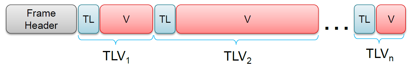
The packet structure consists of fixed sized frame header, followed by variable number of TLVs (see Figure below). Each TLV has fixed header followed by variable size payload. The Byte order is Little Endian.
The frame header is of fixed size (40bytes). It is defined by the structure as
The TLV structure consists of a fixed header, TL (8bytes) followed by TLV specific payload. The TLV header structure is shown below.
The demo outputs point cloud data in floating point format.
The point cloud data are sent using two TLV elements, first one with the detected point cartesian coordinates and the radial velocity, and the second one, this side information, the detected point snr and noise.
The single point is defined as:
The single point side info is defined as:
This demo sends the range profile. This TLV contains the range profile, specified as an array of 16-bit unsigned linear values of range bins. The length is equal to number of range bin elements, (half of the range FFT size, since the ADC samples are real).
This TLV contains the range-Doppler detection matrix (heatmap) which consists of two-dimensional array of 16-bit unsigned magnitude values. The matrix is arranged as X[rangeInd* numDopplerBins + dopplerInd], rangeInd = 0, numRangeBins - 1, dopplerInd = 0, numDopplerBins – 1
This TLV contains statistics described in the structure below.
This TLV contains the output of Rx channel compensation measurement procedure.
Below is the high level flow diagram of Motion and Presence detection OOB demo in Low Power Mode:

Syscfg of Power driver provides some options to be configured by user as per their demo implementations:
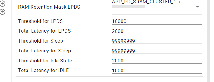
Threshold Value The idle time available only after which entry to various power modes is considered. This is upto the user to configure based on their system requirements.
Latency Value: There is a latency for the device to transition into the different low power modes, and to wake from that specific low power mode to resume activity. The actual transition latency will depend upon overall device state, as well as execution of notification functions that are registered with the Power driver. User is expected to measure this in their implementations and configure this value. If there is Xms idle time, device will get into low power state for (X - Latency value) time duration.
Threshold and latency values can be changed (tuned) to meet specific application requirements. Threshold and Latency values for different power modes can be configured in Power Syscfg:
Enabling wake-up sources from LPDS state: Wake-up from Deep sleep exit is provisioned in the device through a number of external wakeup sources like UART/SPI/GPIO/SYNC_IN/Sleep counter, etc. By Default wake-up using Sleep Counter is enabled in Demo.
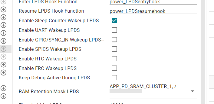
In Low Power Mode SRAM Regions can be retained. Following SRAM Clusters are retained during LPDS:
MMWAVE-L-SDK OOB (out-of-box) demo supports raw ADC data streaming through the LVDS interface. When the radar EVM board connected with the DCA1000EVM board, users can use the DCA1000EVM CLI application to capture the raw data without starting the mmWaveStudio GUI interface. The DCA1000EVM CLI application is primarily a command line tool for configuration of FPGA and recording based on the user inputs. The DCA1000EVM CLI application connects to DCA1000EVM system through 1GB Ethernet for configuration and recording of data. RADAR EVM is connected to DCA1000EVM for data capture and connected to PC for configuration of data generation. However, there are some important limitations associated with this feature:
The DCA1000EVM CLI application is provided for Windows and can be recompiled for other platforms. Users can find the source code and user guide in MMWAVE-STUDIO release package.
The DCA1000EVM CLI application has the following functionalities.
Initiate the power on sequence by turning on the radar EVM first, followed by the DCA1000EVM board. For shutdown, power off the DCA1000EVM board first, and then the radar EVM board.
Please refer to Monitors for details on how to use monitors.
For successful recording of data from RADAR EVM sequence is given as follows
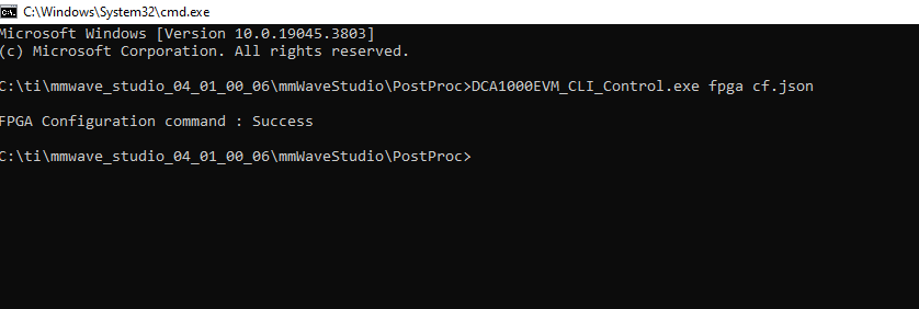
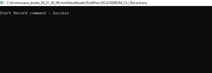
Refer TI_DCA1000EVM_CLI_Software_UserGuide.pdf document for more details.
The path ${SDK_INSTALL_PATH}/tools/ADC_parser includes parsing and post processing scripts for interpreting Raw ADC data acquired from the DCA1000EVM board.
The MmWave Demo supports streaming of raw ADC data over SPI interface every frame during the frame idle time. However, there are some important limitations associated with this feature:
Demos in SDK have this feature disabled by default. Follow below steps to enable this feature in demo.
The path ${SDK_INSTALL_PATH}/tools/ADC_parser includes parsing and post processing scripts for interpreting Raw ADC data acquired through SPI.
When this feature is enabled, the CLI task is removed, and the demo automatically uses the configuration specified in the GRadarCmdString structure within mmw_cli.c to generate the point cloud, eliminating the need for user-provided CLI input. This feature is disabled by default.
To enable this feature, set the CLI_BYPASS macro to 1 in the mmw_cli.h file. To modify the configuration, update the GRadarCmdString structure within mmw_cli.c and adjust the MAX_RADAR_CMD macro in the mmw_cli.h file based on the number of radar commands used.
By default, the Out-of-Box (OOB) demo is configured to set:
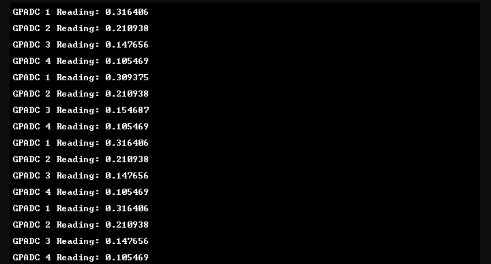
The OOB demo enables external voltage measurements through GPADC. It includes four GPADC channels, each supporting a distinct external voltage measurement. The GPADC operates with unbuffered voltage, has an input range of 0–1.8V, and a resolution of 0.007V. Example GPADC prints from UARTB are shown in the figure below. For more details on enabling GPADC channels, refer Sensor front-end parameters (gpAdcMeasConfig cli command).
Following are power numbers with SDK default configurations measured using INA228 sensor.
| Configuration | Average Power (mW) |
|---|---|
| profile_4T4R_tdm.cfg | 47.6mW |
| profile_3T4R_tdm.cfg | 45.6mW |
| profile_2T4R_bpm.cfg | 48.6mW |
 1.8.20