|
CC26xx Driver Library
|
|
CC26xx Driver Library
|
Functions | |
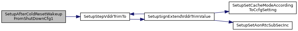
| void | SetupAfterColdResetWakeupFromShutDownCfg1 (uint32_t ccfg_ModeConfReg) |
| First part of configuration required after cold reset and when waking up from shutdown. More... | |
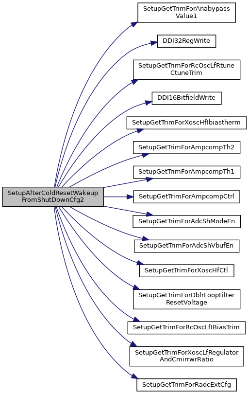
| void | SetupAfterColdResetWakeupFromShutDownCfg2 (uint32_t ui32Fcfg1Revision, uint32_t ccfg_ModeConfReg) |
| Second part of configuration required after cold reset and when waking up from shutdown. More... | |
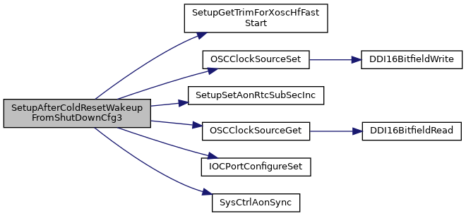
| void | SetupAfterColdResetWakeupFromShutDownCfg3 (uint32_t ccfg_ModeConfReg) |
| Third part of configuration required after cold reset and when waking up from shutdown. More... | |
| uint32_t | SetupGetTrimForAdcShModeEn (uint32_t ui32Fcfg1Revision) |
| Returns the trim value from FCFG1 to be used as ADC_SH_MODE_EN setting. More... | |
| uint32_t | SetupGetTrimForAdcShVbufEn (uint32_t ui32Fcfg1Revision) |
| Returns the trim value from FCFG1 to be used as ADC_SH_VBUF_EN setting. More... | |
| uint32_t | SetupGetTrimForAmpcompCtrl (uint32_t ui32Fcfg1Revision) |
| Returns the trim value to be used for the AMPCOMP_CTRL register in OSC_DIG. More... | |
| uint32_t | SetupGetTrimForAmpcompTh1 (void) |
| Returns the trim value to be used for the AMPCOMP_TH1 register in OSC_DIG. More... | |
| uint32_t | SetupGetTrimForAmpcompTh2 (void) |
| Returns the trim value to be used for the AMPCOMP_TH2 register in OSC_DIG. More... | |
| uint32_t | SetupGetTrimForAnabypassValue1 (uint32_t ccfg_ModeConfReg) |
| Returns the trim value to be used for the ANABYPASS_VALUE1 register in OSC_DIG. More... | |
| uint32_t | SetupGetTrimForDblrLoopFilterResetVoltage (uint32_t ui32Fcfg1Revision) |
| Returns the trim value from FCFG1 to be used as DBLR_LOOP_FILTER_RESET_VOLTAGE setting. More... | |
| uint32_t | SetupGetTrimForRadcExtCfg (uint32_t ui32Fcfg1Revision) |
| Returns the trim value to be used for the RADCEXTCFG register in OSC_DIG. More... | |
| uint32_t | SetupGetTrimForRcOscLfIBiasTrim (uint32_t ui32Fcfg1Revision) |
| Returns the FCFG1 OSC_CONF_ATESTLF_RCOSCLF_IBIAS_TRIM. More... | |
| uint32_t | SetupGetTrimForRcOscLfRtuneCtuneTrim (void) |
| Returns the trim value to be used for the RCOSCLF_RTUNE_TRIM and the RCOSCLF_CTUNE_TRIM bit fields in the XOSCLF_RCOSCLF_CTRL register in OSC_DIG. More... | |
| uint32_t | SetupGetTrimForXoscHfCtl (uint32_t ui32Fcfg1Revision) |
| Returns the trim value to be used for the XOSCHFCTL register in OSC_DIG. More... | |
| uint32_t | SetupGetTrimForXoscHfFastStart (void) |
| Returns the trim value to be used as OSC_DIG:CTL1.XOSC_HF_FAST_START. More... | |
| uint32_t | SetupGetTrimForXoscHfIbiastherm (void) |
| Returns the trim value to be used for the XOSC_HF_IBIASTHERM bit field in the ANABYPASS_VALUE2 register in OSC_DIG. More... | |
| uint32_t | SetupGetTrimForXoscLfRegulatorAndCmirrwrRatio (uint32_t ui32Fcfg1Revision) |
| Returns XOSCLF_REGULATOR_TRIM and XOSCLF_CMIRRWR_RATIO as one packet spanning bits [5:0] in the returned value. More... | |
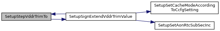
| static int32_t | SetupSignExtendVddrTrimValue (uint32_t ui32VddrTrimVal) |
| Sign extend the VDDR_TRIM setting (special format ranging from -10 to +21) More... | |
| void | SetupSetCacheModeAccordingToCcfgSetting (void) |
| Set correct VIMS_MODE according to CCFG setting (CACHE or GPRAM) More... | |
| void | SetupSetAonRtcSubSecInc (uint32_t subSecInc) |
| Doing the tricky stuff needed to enter new RTCSUBSECINC value. More... | |
| void | SetupStepVddrTrimTo (uint32_t toCode) |
| Set VDDR boost mode (by setting VDDR_TRIM to FCFG1..VDDR_TRIM_HH and setting VDDS_BOD to max) More... | |
This module contains functions from the Setup API which are likely to be in ROM.
| void SetupAfterColdResetWakeupFromShutDownCfg1 | ( | uint32_t | ccfg_ModeConfReg | ) |
First part of configuration required after cold reset and when waking up from shutdown.
Configures the following based on settings in CCFG (Customer Configuration area:
In addition the battery monitor low limit for internal regulator mode is set to a hard coded value.
| ccfg_ModeConfReg | is the value of the CCFG_O_MODE_CONF_1 register |
Referenced by TrimAfterColdResetWakeupFromShutDown().
| void SetupAfterColdResetWakeupFromShutDownCfg2 | ( | uint32_t | ui32Fcfg1Revision, |
| uint32_t | ccfg_ModeConfReg | ||
| ) |
Second part of configuration required after cold reset and when waking up from shutdown.
Configures and trims functionalites required for use of XOSC_HF. The configurations and trimmings are based on settings in FCFG1 (Factory Configuration area) and partly on ccfg_ModeConfReg.
| ui32Fcfg1Revision | is the value of the FCFG1_O_FCFG1_REVISION register |
| ccfg_ModeConfReg | is the value of the CCFG_O_MODE_CONF_1 register |
Referenced by TrimAfterColdResetWakeupFromShutDown().
| void SetupAfterColdResetWakeupFromShutDownCfg3 | ( | uint32_t | ccfg_ModeConfReg | ) |
Third part of configuration required after cold reset and when waking up from shutdown.
Configures the following:
ccfg_ModeConfReg. If HPOSC is selected on a HPOSC device the oscillator is configured based on settings in FCFG1 (Factory Configuration area).ccfg_ModeConfReg.| ccfg_ModeConfReg | is the value of the CCFG_O_MODE_CONF_1 register |
Referenced by TrimAfterColdResetWakeupFromShutDown().
| uint32_t SetupGetTrimForAdcShModeEn | ( | uint32_t | ui32Fcfg1Revision | ) |
Returns the trim value from FCFG1 to be used as ADC_SH_MODE_EN setting.
| ui32Fcfg1Revision | is the value of the FCFG1_O_FCFG1_REVISION register |
Referenced by SetupAfterColdResetWakeupFromShutDownCfg2().
| uint32_t SetupGetTrimForAdcShVbufEn | ( | uint32_t | ui32Fcfg1Revision | ) |
Returns the trim value from FCFG1 to be used as ADC_SH_VBUF_EN setting.
| ui32Fcfg1Revision | is the value of the FCFG1_O_FCFG1_REVISION register |
Referenced by SetupAfterColdResetWakeupFromShutDownCfg2().
| uint32_t SetupGetTrimForAmpcompCtrl | ( | uint32_t | ui32Fcfg1Revision | ) |
Returns the trim value to be used for the AMPCOMP_CTRL register in OSC_DIG.
| ui32Fcfg1Revision | is the value of the FCFG1_O_FCFG1_REVISION register |
Referenced by SetupAfterColdResetWakeupFromShutDownCfg2().
| uint32_t SetupGetTrimForAmpcompTh1 | ( | void | ) |
Returns the trim value to be used for the AMPCOMP_TH1 register in OSC_DIG.
Referenced by SetupAfterColdResetWakeupFromShutDownCfg2().
| uint32_t SetupGetTrimForAmpcompTh2 | ( | void | ) |
Returns the trim value to be used for the AMPCOMP_TH2 register in OSC_DIG.
Referenced by SetupAfterColdResetWakeupFromShutDownCfg2().
| uint32_t SetupGetTrimForAnabypassValue1 | ( | uint32_t | ccfg_ModeConfReg | ) |
Returns the trim value to be used for the ANABYPASS_VALUE1 register in OSC_DIG.
| ccfg_ModeConfReg | is the value of the CCFG_O_MODE_CONF_1 register |
Referenced by OSC_AdjustXoscHfCapArray(), and SetupAfterColdResetWakeupFromShutDownCfg2().
| uint32_t SetupGetTrimForDblrLoopFilterResetVoltage | ( | uint32_t | ui32Fcfg1Revision | ) |
Returns the trim value from FCFG1 to be used as DBLR_LOOP_FILTER_RESET_VOLTAGE setting.
| ui32Fcfg1Revision | is the value of the FCFG1_O_FCFG1_REVISION register |
Referenced by SetupAfterColdResetWakeupFromShutDownCfg2().
| uint32_t SetupGetTrimForRadcExtCfg | ( | uint32_t | ui32Fcfg1Revision | ) |
Returns the trim value to be used for the RADCEXTCFG register in OSC_DIG.
| ui32Fcfg1Revision | is the value of the FCFG1_O_FCFG1_REVISION register |
Referenced by SetupAfterColdResetWakeupFromShutDownCfg2().
| uint32_t SetupGetTrimForRcOscLfIBiasTrim | ( | uint32_t | ui32Fcfg1Revision | ) |
Returns the FCFG1 OSC_CONF_ATESTLF_RCOSCLF_IBIAS_TRIM.
| ui32Fcfg1Revision | is the value of the FCFG1_O_FCFG1_REVISION register |
Referenced by SetupAfterColdResetWakeupFromShutDownCfg2().
| uint32_t SetupGetTrimForRcOscLfRtuneCtuneTrim | ( | void | ) |
Returns the trim value to be used for the RCOSCLF_RTUNE_TRIM and the RCOSCLF_CTUNE_TRIM bit fields in the XOSCLF_RCOSCLF_CTRL register in OSC_DIG.
Referenced by SetupAfterColdResetWakeupFromShutDownCfg2().
| uint32_t SetupGetTrimForXoscHfCtl | ( | uint32_t | ui32Fcfg1Revision | ) |
Returns the trim value to be used for the XOSCHFCTL register in OSC_DIG.
| ui32Fcfg1Revision | is the value of the FCFG1_O_FCFG1_REVISION register |
Referenced by SetupAfterColdResetWakeupFromShutDownCfg2().
| uint32_t SetupGetTrimForXoscHfFastStart | ( | void | ) |
Returns the trim value to be used as OSC_DIG:CTL1.XOSC_HF_FAST_START.
Referenced by SetupAfterColdResetWakeupFromShutDownCfg3().
| uint32_t SetupGetTrimForXoscHfIbiastherm | ( | void | ) |
Returns the trim value to be used for the XOSC_HF_IBIASTHERM bit field in the ANABYPASS_VALUE2 register in OSC_DIG.
Referenced by SetupAfterColdResetWakeupFromShutDownCfg2().
| uint32_t SetupGetTrimForXoscLfRegulatorAndCmirrwrRatio | ( | uint32_t | ui32Fcfg1Revision | ) |
Returns XOSCLF_REGULATOR_TRIM and XOSCLF_CMIRRWR_RATIO as one packet spanning bits [5:0] in the returned value.
| ui32Fcfg1Revision | is the value of the FCFG1_O_FCFG1_REVISION register |
Referenced by SetupAfterColdResetWakeupFromShutDownCfg2().
| void SetupSetAonRtcSubSecInc | ( | uint32_t | subSecInc | ) |
Doing the tricky stuff needed to enter new RTCSUBSECINC value.
| subSecInc |
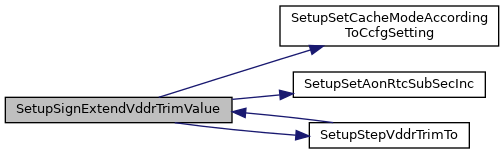
Referenced by OSC_HPOSCRtcCompensate(), SetupAfterColdResetWakeupFromShutDownCfg3(), and SetupSignExtendVddrTrimValue().
| void SetupSetCacheModeAccordingToCcfgSetting | ( | void | ) |
Set correct VIMS_MODE according to CCFG setting (CACHE or GPRAM)
Referenced by SetupSignExtendVddrTrimValue(), and SetupTrimDevice().
|
inlinestatic |
Sign extend the VDDR_TRIM setting (special format ranging from -10 to +21)
| ui32VddrTrimVal |
Referenced by SetupStepVddrTrimTo().
| void SetupStepVddrTrimTo | ( | uint32_t | toCode | ) |
Set VDDR boost mode (by setting VDDR_TRIM to FCFG1..VDDR_TRIM_HH and setting VDDS_BOD to max)
| toCode | specifies the target VDDR trim value. The input parameter toCode can be either the signed extended trim value or holding the trim code bits only. |
Referenced by SetupAfterColdResetWakeupFromShutDownCfg1(), and SetupSignExtendVddrTrimValue().